Introduction
Void formation represents a persistent challenge in the PCB manufacturing process, particularly during the lamination stage where multiple layers of prepreg and copper foil are bonded under heat and pressure. These PCB lamination voids manifest as air pockets or gas inclusions trapped within the laminate structure, potentially undermining the board's integrity. Electric engineers must grasp this phenomenon to ensure reliable performance in high-density interconnects and multilayer designs. Factors such as material properties and process controls directly influence void creation, making proactive management essential. This article delves into the underlying mechanisms of void formation and outlines proven mitigation strategies aligned with industry practices.
What Are PCB Lamination Voids and Why Do They Matter?
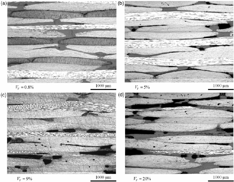
PCB lamination voids are discrete regions of unbonded or gas-filled spaces within the cured laminate, often appearing between copper foils and prepreg layers or embedded in the resin matrix. They arise from incomplete resin flow or trapped gases that fail to escape during pressing. In the PCB manufacturing process, these voids compromise mechanical adhesion, reducing peel strength and increasing susceptibility to delamination under thermal stress. Electric engineers encounter these defects in quality inspections, where they correlate with failures in thermal management and signal integrity.
The significance of addressing void formation cannot be overstated, as voids diminish thermal conductivity by creating insulating barriers that hinder heat dissipation. Mechanical weaknesses from voids accelerate micro-cracking during thermal cycling, potentially leading to conductive anodic filamentation over time. IPC-A-600 provides acceptability criteria for laminate voids, classifying them based on size, location, and density to guide manufacturing conformance. For mission-critical applications, unchecked voids elevate reliability risks, prompting rigorous process controls in production environments.
Mechanisms of Void Formation
Void formation in PCB lamination stems primarily from air entrapment during layer stacking and initial pressing. As prepregs and cores are aligned in the press book, ambient air can become occluded between surfaces if evacuation is insufficient. Rapid application of pressure before adequate flow exacerbates this, squeezing air into isolated pockets that resist escape as resin viscosity increases. Factory observations confirm that uneven layup or surface irregularities on copper foils contribute significantly to these air pockets.
Material outgassing represents another dominant mechanism, where volatile compounds in the resin system vaporize under lamination temperatures typically exceeding 170 degrees Celsius. Prepregs contain solvents, moisture, or uncured oligomers that transition to gas phase, expanding and forming bubbles if not vented. Moisture absorbed during storage is particularly problematic, as it vaporizes into steam, amplifying void size due to the high volume expansion ratio. This outgassing intensifies with higher resin content or low-flow prepregs, common in high-Tg materials for advanced boards.
Process parameters further drive void creation through mismatched heat and pressure profiles. Excessive ramp rates cause premature gelation, trapping gases before full consolidation. Conversely, prolonged low-pressure dwells allow outgassing but risk resin starvation voids from over-flow. Contamination from dust or oils on foils disrupts wetting, fostering weak bonds prone to voiding at interfaces.
Detection and Inspection of Voids
Identifying PCB lamination voids requires non-destructive techniques integrated into the manufacturing workflow. Ultrasonic C-scan imaging excels at mapping internal voids by detecting acoustic impedance mismatches between resin and gas. Cross-sectioning followed by optical or scanning electron microscopy provides definitive confirmation, revealing void morphology and distribution. These methods align with factory quality control, enabling early detection post-lamination.
Electrical testing, such as impedance analysis, indirectly flags voids through variations in dielectric uniformity. Thermal imaging during simulated loads highlights hotspots from void-induced poor conductivity. Adopting these inspections ensures compliance with performance specifications, preventing field failures.
Mitigation Strategies for Void Formation
Vacuum lamination stands as a cornerstone for void mitigation, employing reduced pressure chambers to evacuate air pockets and outgassing products prior to full consolidation. By drawing a vacuum of 20 to 50 torr during initial dwell, gases migrate to vents before resin gelation locks them in place. This technique proves especially effective for thick multilayers or high-resin stacks, yielding void-free laminates in production runs.
Pre-baking prepregs and cores removes absorbed moisture, curtailing steam-induced voids as per IPC-1601 guidelines for handling and storage. Baking at controlled temperatures around 100 to 125 degrees Celsius for several hours achieves moisture levels below 0.5 percent, minimizing outgassing risks. Proper material storage in dry cabinets maintains this preconditioning, a factory best practice for consistent results.
Optimizing press cycles through gradual heat ramps and staged pressure application facilitates controlled resin flow and degassing. Initial low-pressure soaks allow volatiles to escape, followed by ramped pressure to 300 to 500 psi for bonding. Low-flow prepregs demand finer tuning to avoid starvation, while surface treatments on copper enhance wetting.
Material selection plays a pivotal role in void mitigation, favoring low-outgassing resins with high resin-to-glass ratios for better flow. Factory-driven insights emphasize qualifying laminates per IPC-6012 performance specs, ensuring compatibility with process windows. Cleanroom protocols eliminate contaminants, preventing adhesion defects that seed voids.
Best Practices in the PCB Manufacturing Process
Implementing a holistic void mitigation protocol begins with supplier qualification for prepreg consistency, including flow and gel time verification. Factory layouts should incorporate automated layup to minimize handling-induced air entrapment. Real-time process monitoring via press-embedded sensors tracks temperature uniformity, averting hot spots that trigger localized outgassing.
Post-lamination, flatness checks and burn-in tests simulate operational stresses, exposing latent voids early. Data logging across runs enables continuous improvement, correlating parameters to void rates. These practices, rooted in standard conformance, elevate yield and reliability for electric engineers specifying boards.
Conclusion
Understanding void formation mechanisms, from air entrapment and material outgassing to process mismatches, equips electric engineers to safeguard PCB reliability. Mitigation through vacuum lamination, pre-baking, and optimized cycles directly addresses these root causes in the manufacturing process. Adhering to standards like IPC-A-600 and IPC-6012 ensures defect-free laminates, supporting robust designs. By integrating these factory insights, production teams minimize air pockets, enhancing thermal and mechanical performance across applications.
FAQs
Q1: What causes PCB lamination voids in the manufacturing process?
A1: PCB lamination voids primarily result from air entrapment during layup, material outgassing under heat, and moisture vaporization in prepregs. Inadequate vacuum or rapid pressure ramps trap gases before resin flow completes bonding. Factory controls focus on these mechanisms to maintain laminate integrity per IPC standards.
Q2: How does vacuum lamination aid in void mitigation?
A2: Vacuum lamination applies reduced pressure to extract air pockets and volatiles from the stack before gelation, significantly reducing void formation. This process suits multilayer boards prone to outgassing, achieving near-zero critical voids. Electric engineers specify it for high-reliability builds in demanding environments.
Q3: What role does material outgassing play in void formation?
A3: Material outgassing releases solvents and moisture as gases during lamination heating, forming bubbles if not vented. Pre-baking per IPC-1601 guidelines removes these volatiles, preventing steam expansion. Consistent storage and low-outgas resins further mitigate this in production.
Q4: Can voids be completely eliminated in PCB lamination?
A4: While zero voids represent the target, complete elimination depends on process precision and material quality. Vacuum techniques and controlled cycles minimize them to acceptable levels under IPC-A-600 criteria. Ongoing monitoring ensures sustained low void rates in manufacturing.
References
IPC-A-600K — Acceptability of Printed Boards. IPC, 2020
IPC-6012E — Qualification and Performance Specification for Rigid Printed Boards. IPC, 2017
IPC-1601A — Printed Board Handling and Storage Guidelines. IPC, 2018


