Introduction
In the fast-paced world of PCB prototypes development, rework is a routine part of the process as engineers iterate on designs to meet performance goals. Prototype PCBs often undergo multiple soldering cycles during testing and validation, which can introduce hidden defects not visible through optical inspection. X-Ray Inspection emerges as a critical tool in the X-Ray Inspection Prototype PCB Rework workflow, enabling non-destructive analysis of internal structures. This method allows engineers to verify solder joint integrity beneath components like BGAs and QFNs, where traditional visual checks fall short. By integrating X-Ray Inspection into the rework process, teams reduce failure risks in subsequent assembly stages and ensure reliability from the outset. For electric engineers handling PCB prototypes, mastering this technique translates to fewer iterations and accelerated time-to-market.
What Is X-Ray Inspection and Why It Matters for Prototype PCB Rework
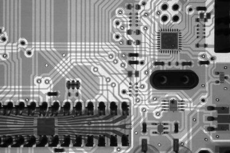
X-Ray Inspection involves directing low-energy X-rays through the PCB to produce images based on material density differences, highlighting solder joints and vias without disassembly. In prototype PCB rework, this becomes essential because hand soldering or reflow processes on small batches often lead to inconsistencies that compromise functionality. Unlike automated optical inspection suited for surface features, X-Ray Inspection penetrates multi-layer boards to expose subsurface issues, making it indispensable for soldering prototypes. Factory-driven quality control relies on it to confirm rework success, preventing costly respins. Engineers benefit from its ability to quantify joint quality, aligning with production standards early in development. Ultimately, incorporating X-Ray Inspection Prototype PCB Rework minimizes downtime and supports precise troubleshooting in high-mix, low-volume environments.
Technical Principles of X-Ray Inspection in PCBs
X-rays generate 2D or 3D images by passing through the board, where denser materials like solder absorb more radiation and appear brighter, while voids show as darker areas. Transmission X-ray systems provide real-time oblique views, ideal for assessing BGA ball attachment and via fill in prototypes. Oblique-angle imaging reveals fillet formation and bridging under components, critical for rework validation. Automated X-ray systems use software algorithms to detect anomalies like insufficient solder volume or cracks based on grayscale thresholds. This principle ensures comprehensive coverage of hidden features, from through-hole barrels to bottom-side terminations. In PCB prototypes, where layer counts vary, adjustable kV and filtration settings optimize contrast for accurate defect identification.
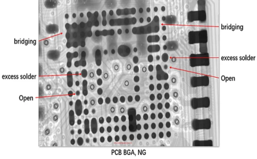
Common defects detected include voids exceeding acceptable limits, which weaken mechanical strength and thermal conductivity. Solder bridges create shorts, while head-in-pillow defects mimic proper joints externally but fail internally. Misalignment in fine-pitch devices shifts balls, risking opens during thermal cycling. Insufficient wetting leaves unfilled interfaces, and cracks propagate under stress. These issues, prevalent in soldering prototypes due to manual handling, demand X-Ray Inspection for reliable diagnosis.
Common Defects in Soldering Prototypes Detected by X-Ray Inspection
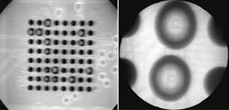
Soldering prototypes frequently suffer from voids formed by outgassing during reflow, visible as dark spots in X-ray images that indicate trapped flux or moisture. These reduce heat dissipation and increase electrical resistance, common in prototypes rushed through quick-turn processes. Bridging occurs when excess solder connects adjacent pads, appearing as continuous bright lines that short circuits. Head-in-pillow defects show partial ball collapse against pads, mimicking alignment but lacking intermetallic bonds. Component shift during rework manifests as offset shadows, especially in dense BGA arrays. Factory insights reveal that X-Ray Inspection catches over 90% of such hidden flaws missed by visual means, guiding targeted fixes.
Insufficient solder volume presents as undersized or asymmetric balls, failing to meet joint criteria. Cracks in solder or vias appear as linear dark lines, exacerbated by thermal mismatch in prototypes. Tombstoning in chip components tilts shadows, indicating uneven wetting. Pad lifting detaches traces, showing gaps in layer interfaces. By systematically scanning these, engineers prioritize rework, enhancing prototype yield.
Integrating X-Ray Inspection into the Rework Process
Begin the rework process with pre-inspection X-Ray scans to baseline defects, focusing on targeted areas like reworked BGAs. After desoldering and cleaning, perform a quick scan to confirm residue removal and pad integrity. Post-rework, full X-Ray Inspection verifies new joint formation, checking for voids and alignment per IPC J-STD-001 guidelines for soldered assemblies. This sequential approach aligns factory workflows, reducing escape defects to downstream testing. For PCB prototypes, limit exposure times to under 30 seconds per view to maintain throughput. Document findings with annotated images for design feedback loops.
In multi-layer prototypes, use 3D X-ray for via inspection, rotating the board to capture cross-sections. Calibrate systems daily for consistent grayscale, ensuring repeatability across shifts. Combine with thermal profiling to correlate reflow parameters with joint quality. This integration streamlines soldering prototypes rework, cutting cycle times by focusing efforts on verified issues.
Best Practices for X-Ray Inspection in Prototype PCB Rework
Position the PCB prototype securely in the fixture to minimize artifacts from movement, using low-dose settings for operator safety. Select magnification based on pitch size, with 10x for fine-pitch under 0.5mm. Train operators to interpret images against IPC-A-610 acceptability criteria, distinguishing class 2 from class 3 requirements. Archive scans with timestamps for traceability in rework iterations. For soldering prototypes, inspect 100% of high-risk joints like BGAs, sampling others statistically.
Avoid common pitfalls by maintaining equipment cleanliness to prevent false shadows, and cross-verify with electrical testing. Update software for advanced defect recognition, improving detection of subtle cracks. In factory settings, integrate X-Ray Inspection Prototype PCB Rework stations post-reflow and pre-functional test. Collaborate with design teams to refine land patterns based on recurrent findings. These practices ensure robust prototypes ready for volume ramp-up.
Troubleshooting Rework Issues with X-Ray Insights
When voids persist post-rework, X-ray reveals flux entrapment; extend preheat to evaporate volatiles. Bridges indicate stencil misalignment; refine apertures for prototypes. Misaligned balls signal vibration during reflow; secure fixtures better. Head-in-pillow defects point to pad finish incompatibility; test ENIG versus HASL. Cracks suggest excessive force in desoldering; adopt hot air over conduction tools.
Layered analysis in X-ray pinpoints via barrel voids from plating inconsistencies. Electrical opens correlate with insufficient volume shadows. By mapping defects to process steps, engineers refine soldering prototypes techniques iteratively. Factory data shows this targeted troubleshooting boosts first-pass yield significantly.
Conclusion
X-Ray Inspection stands as a cornerstone in Prototype PCB Rework, offering unparalleled visibility into solder integrity for reliable outcomes. Electric engineers leveraging its principles detect voids, bridges, and misalignments that plague soldering prototypes, aligning with standards like IPC J-STD-001 and IPC-A-610. Best practices in integration and troubleshooting minimize rework cycles, accelerating prototype validation. Factory-driven adoption ensures quality scales to production seamlessly. Prioritizing this non-destructive method empowers precise decision-making, reducing risks in PCB prototypes development.
FAQs
Q1: What is X-Ray Inspection for PCB prototypes?
A1: X-Ray Inspection for PCB prototypes uses penetrating radiation to image internal solder joints and vias non-destructively. It excels in prototype rework by revealing hidden defects like voids and bridges invisible to optical methods. Factory teams apply it post-soldering to verify rework process quality, ensuring joints meet performance needs without disassembly. This approach supports rapid iterations in development cycles.
Q2: Why is X-Ray Inspection essential in the rework process for soldering prototypes?
A2: In the rework process for soldering prototypes, X-Ray Inspection confirms joint integrity after modifications, catching issues like insufficient solder or misalignment. Prototypes often face manual handling risks, amplifying defects. It guides precise fixes, aligning with IPC standards for acceptability. Engineers rely on it to prevent field failures early.
Q3: How does X-Ray Inspection Prototype PCB Rework improve quality control?
A3: X-Ray Inspection Prototype PCB Rework enhances quality control by quantifying solder volume and detecting subsurface flaws in real-time. For PCB prototypes, it verifies BGA attachments and via fill post-rework. Factory insights from scans inform process tweaks, boosting yield. Consistent use ensures compliance with soldering standards.
Q4: What common defects does X-Ray Inspection detect in PCB prototypes?
A4: X-Ray Inspection detects voids, bridges, head-in-pillow defects, and cracks in PCB prototypes solder joints. These arise from reflow inconsistencies in soldering prototypes. Images highlight misalignment and insufficient wetting for targeted rework. It provides factory-level precision beyond surface inspections.
References
IPC J-STD-001H — Requirements for Soldered Electrical and Electronic Assemblies. IPC, 2018
IPC-A-610H — Acceptability of Electronic Assemblies. IPC, 2019
IPC-7711/7721B — Rework, Modification and Repair of Electronic Assemblies. IPC, 2020


