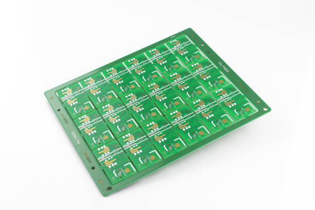
What Defines a Four-Layer Printed Circuit Board?
A four-layer printed circuit board (PCB) represents a significant advancement over simpler two-layer designs, offering a sophisticated structure that balances performance, cost, and spatial efficiency. Unlike a basic two-layer board, this configuration incorporates four distinct copper layers, each separated by insulating dielectric materials. This construction makes it a preferred choice for electronics demanding moderate to high complexity, robust signal integrity, and dependable power delivery.
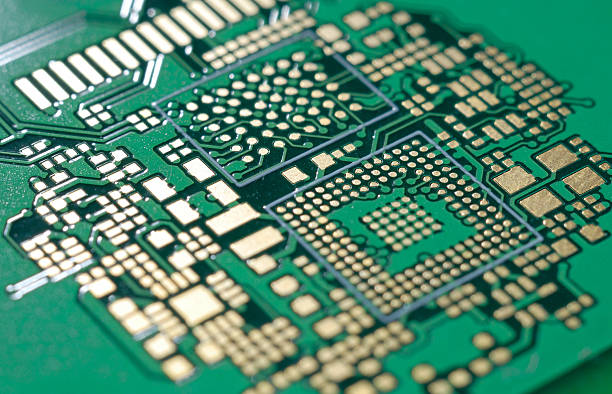
The typical composition of a four-layer PCB includes two outer layers and two inner layers. The outer layers, designated as the top and bottom, are primarily used for mounting components and routing signal traces. The inner layers usually function as dedicated power and ground planes, which are crucial for providing low-resistance return paths for signals and effective shielding against electromagnetic interference (EMI).
Why Are Four-Layer PCBs So Widely Used?
The widespread adoption of four-layer PCBs in contemporary electronics stems from their ability to deliver a compelling blend of technical advantages and commercial viability. This layered structure significantly enhances routing density compared with other types of PCBs, such as two-layer boards, while remaining more cost-effective than PCBs with six or eight layers.
Key Benefits of Four-Layer Boards
● Reduced Electromagnetic Interference (EMI): The presence of dedicated power and ground planes acts as an internal shield, effectively minimizing unwanted radiated noise.
● Enhanced Signal Integrity: Continuous reference planes within the four-layer structure help to reduce impedance discontinuities and prevent crosstalk between signals.
● Compact Designs: The ability to route signals densely across multiple layers enables the creation of smaller, more compact electronic devices, which is critical for space-constrained applications.
● Improved Power Delivery: A dedicated inner plane ensures a stable and efficient distribution of voltage and current throughout the board.
● Cost-Effectiveness for Complexities: Offering superior capabilities over two-layer boards, yet remaining more economical than higher-layer alternatives, the four layer PCB hits a "sweet spot" for many electronic products requiring a balance of performance and budget.
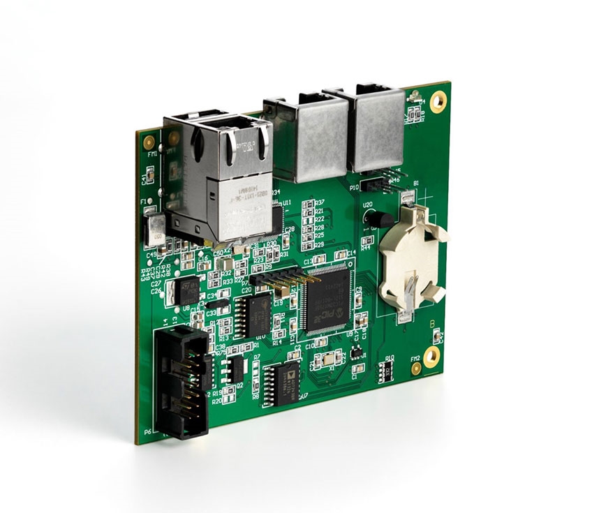
Where Are Four-Layer PCBs Most Frequently Applied?
The balanced combination of cost, performance, and compact size makes four-layer PCBs exceptionally versatile, suitable for a broad spectrum of industries and applications.
Common Applications
● Industrial Control Systems: Used in various controllers, programmable logic controllers (PLCs), and automation modules.
● IoT Devices and Sensors: Powering smart home devices, wearable technology, and remote sensing units.
● Automotive Electronics: Integrated into Engine Control Units (ECUs), infotainment systems, and driver-assist modules.
● Consumer Electronics: Found in everyday devices such as smartphones, laptops, tablets, and gaming hardware.
● Communication Equipment: Essential for routers, radio frequency (RF) devices, and various wireless communication modules.
Across these diverse sectors, the four-layer PCB design facilitates the creation of compact yet robust electronic solutions.
What Are the Fundamental Principles of Four-Layer PCB Design?
When embarking on the design of a four-layer board, engineers adhere to specific principles to optimize functionality and manufacturability. These guidelines are crucial for ensuring the final product meets performance expectations.
Core Design Strategies
● Inner Layer Utilization: Dedicating inner layers to power and ground planes is a standard practice to minimize noise and ensure continuous reference paths for signals.
● Outer Layer Functions: The outer layers are typically reserved for component placement and signal traces, providing easy access for assembly and rework.
● Surface Mount Device (SMD) Routing: With components mounted on the surface, many traces can be routed efficiently without the need for numerous vias, thereby simplifying the board's complexity.
● Electromagnetic Interference (EMI) Control: To mitigate radiation, it is essential to keep signal return paths as short as possible and in close proximity to their respective reference planes.
● Design Balance: A well-executed four-layer PCB design meticulously balances considerations like manufacturability, cost implications, and overall performance.
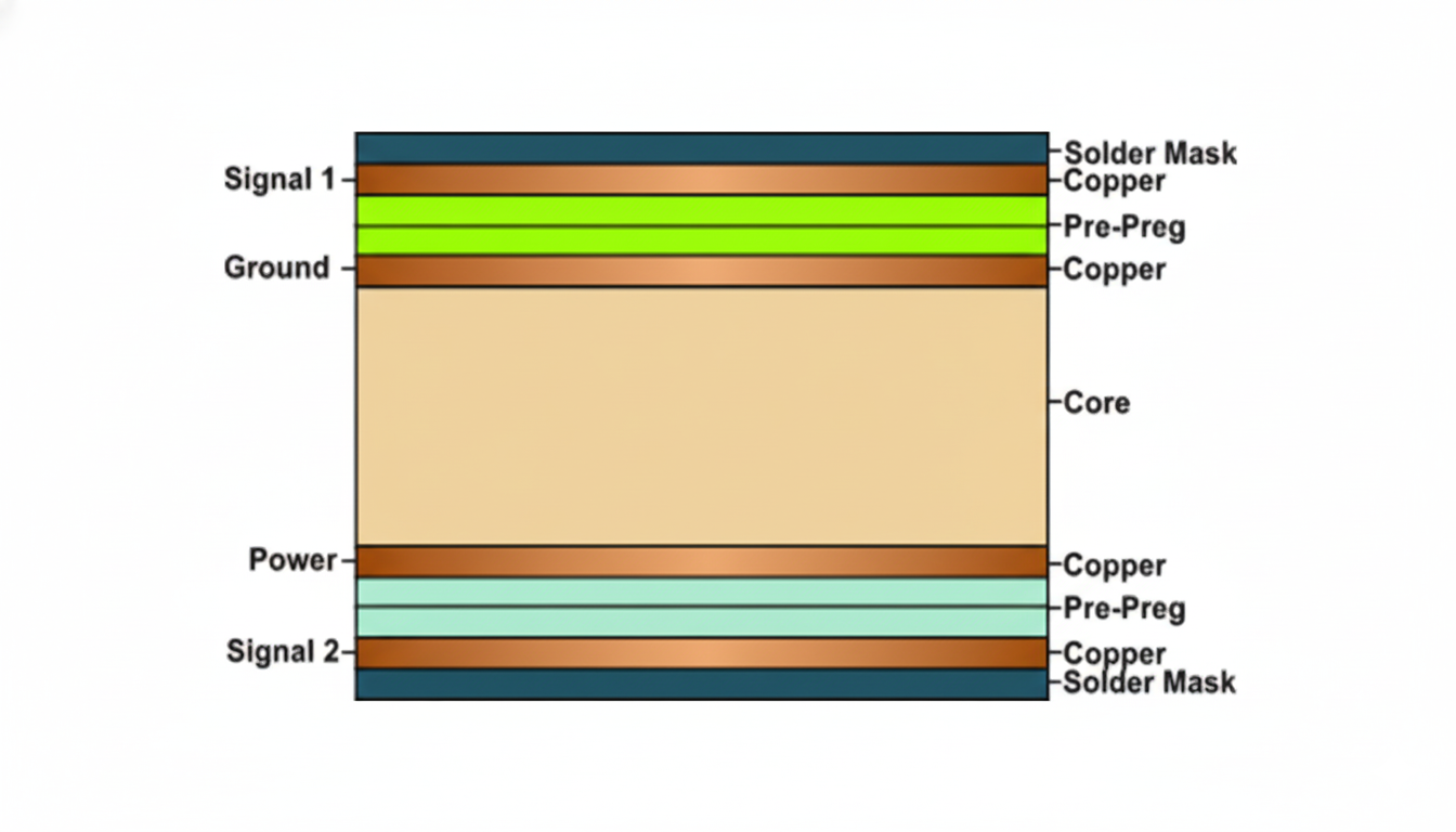
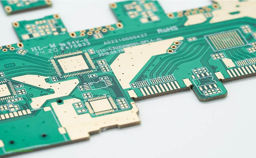
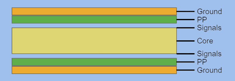
What Are the Standard Four-Layer PCB Stackup Configurations?
The "stackup" refers to the specific arrangement of copper and dielectric layers within a four-layer PCB. The chosen stackup configuration directly influences crucial factors such as EMI reduction, signal integrity, and the ease of manufacturing.
Common Stackup Options
● Signals-Ground-VCC-Signals: This is a widely used standard stackup. The specific assignment of Ground (GND) and Voltage Common Collector (VCC) can be switched between the inner layers, often based on which layer carries more signal traces.
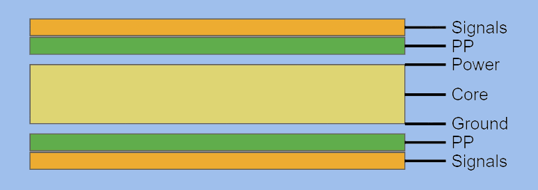
● Ground-Signals-Signals-Ground: Another popular configuration, particularly beneficial for high-speed designs where having solid ground planes on both inner layers provides excellent shielding and signal integrity.
Deciding on the Right Stackup
The selection of a specific four-layer PCB stackup depends on several critical factors:
● High-speed designs often benefit from configurations like ground–signal–signal–ground due to superior signal integrity.
● Cost-sensitive designs may favor a signal–ground–power–signal arrangement for efficiency.
● Power delivery requirements can dictate the need for thicker planes or higher copper weights to ensure stable voltage and current.
By carefully choosing the appropriate four-layer PCB stackup, designers can guarantee optimal electrical and thermal performance for their applications.
Suggested Reading: Designing a 4-Layer PCB Stackup: Enhancing Signal Integrity and Performance
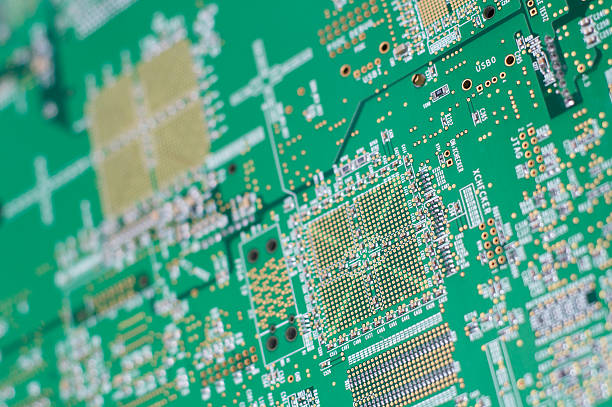
What Are the Key Routing Principles for Four-Layer PCBs?
Effective routing is paramount in four-layer PCB design to ensure both reliability and manufacturability. Adhering to specific principles helps manage signal integrity, power delivery, and EMI.
Essential Routing Guidelines
● Priority Routing: Critical signals such as clocks, differential pairs, and other high-speed lines should be routed with top priority.
● Signal Layering: Sensitive signals should always be routed in close proximity to their corresponding ground planes.
● Avoiding Plane Splits: Traces should never be routed across split planes, as this can interrupt return paths and degrade signal integrity.
● Loop Area Minimization: Keeping signal loops as small as possible effectively reduces EMI emissions.
● Length Matching: This is especially crucial for differential pairs and clock lines to maintain signal synchronization.
● Spacing Control: Adequate spacing between traces is necessary to prevent crosstalk, particularly between fast and slow signals.
● Impedance Matching: All transmission lines must be designed to match the specified impedance requirements.
● Power Routing: Power traces should be designed with sufficient width to handle the required current-carrying capacity.
● Via Management: The number of vias should be limited to reduce parasitic capacitance and inductance; for high-speed lines, back-drilling may be considered.
● Manufacturer Rules Adherence: Always align design rules with the fabrication capabilities of the chosen manufacturer, such as AIVON.
Advanced Routing Techniques for High-Density Four-Layer Boards
As electronic devices continue to miniaturize, four-layer PCB designs frequently encounter significant routing challenges. Advanced strategies are essential to overcome these hurdles and maintain high performance.
Strategies for Complex Designs
● Length Tuning: Precisely matching trace lengths is vital for ensuring synchronized high-speed signals.
● Differential Pair Routing: This involves controlled impedance routing specifically for pairs like USB, HDMI, or PCIe.
● Stub Minimization: Reducing trace stubs is critical for improving overall signal integrity by preventing reflections.
● Crosstalk Mitigation: Employing strategic trace spacing and ground shielding helps to minimize unwanted signal coupling.
Best Practices for Via Placement in Four-Layer Designs
The placement of vias within a four-layer board directly impacts its electrical performance. Careful consideration is required to minimize undesirable parasitic effects.
Optimal Via Usage
● Limiting Transitions: Excessive use of vias can increase parasitic capacitance and inductance, so their number should be managed.
● Via-in-Pad Technology: This technique can enhance high-frequency performance but typically comes with increased manufacturing costs.
● Back-Drilling: Used to remove unused portions of via barrels (stubs), which helps in reducing signal reflections in high-speed applications.
● Stitching Vias: These are strategically placed vias that help maintain continuous reference planes and improve EMI shielding across different layers.
Suggested Reading: Optimizing Via Placement in 4-Layer PCBs: A Design Guide
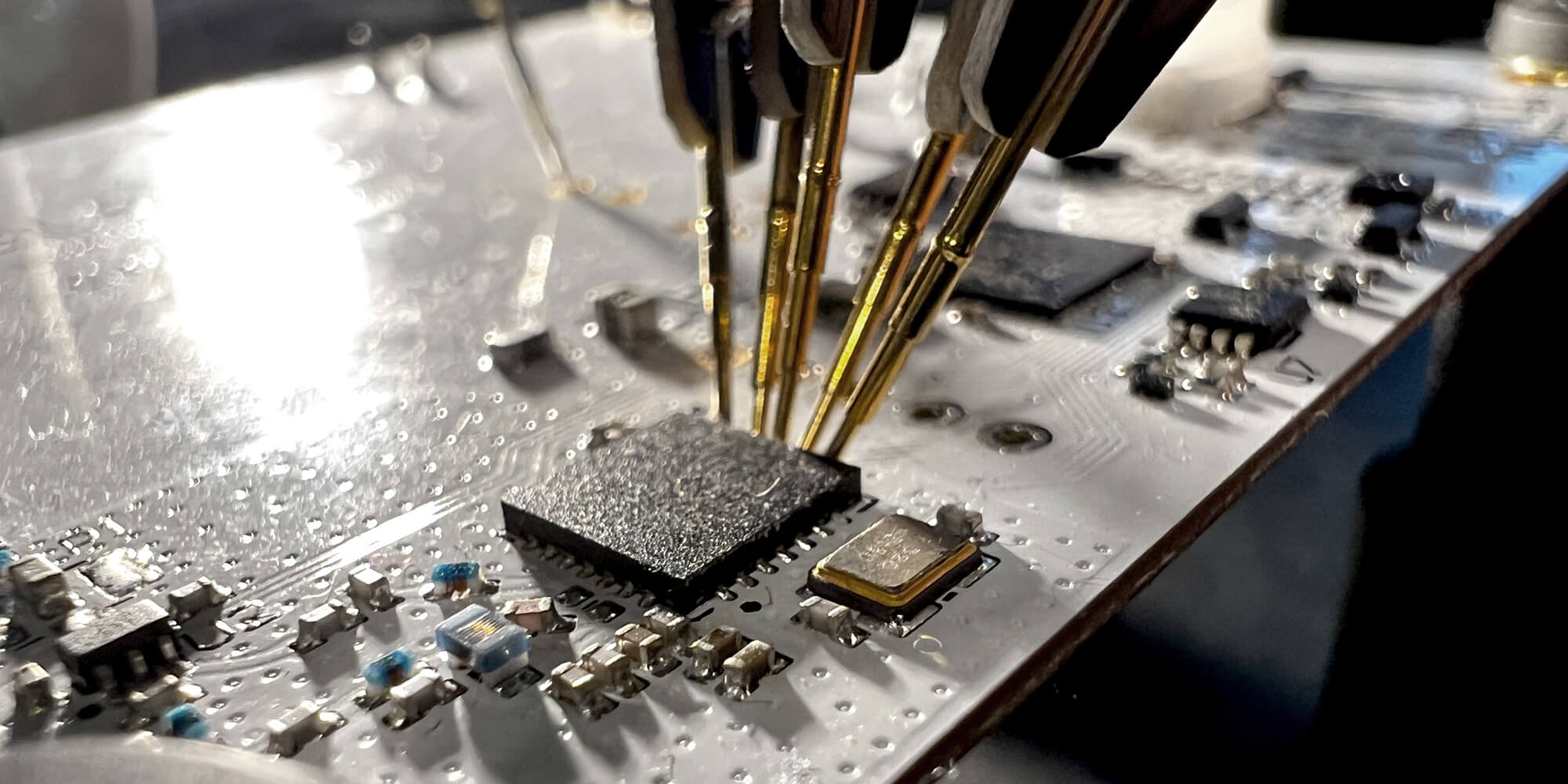
The Manufacturing Process for Four-Layer PCBs
AIVON offers reliable manufacturing services for four-layer PCBs, with a range of customizable options to meet diverse project requirements.
AIVON's Standard 4-Layer PCB Offerings
● Customizable Thickness: Options are available for various board thicknesses, such as 1.6mm or 2.0mm.
● Copper Weight for Outer Layers: Standard choices include 1 oz or 2 oz copper.
● Copper Weight for Inner Layers: Typically 0.5 oz or 1 oz copper.
● Substrate Materials: Both standard FR4 and high-Tg (glass transition temperature) substrates are available to suit different thermal demands.
AIVON also provides comprehensive Design for Manufacturability (DFM) analysis and stackup consultation. This ensures that your four-layer PCB design not only meets performance specifications but is also optimized for efficient and high-quality production.
Why Consider AIVON for Your Four-Layer PCB Needs?
Choosing AIVON as your manufacturing partner for four-layer boards offers numerous advantages, from rapid production to expert support and competitive pricing.
AIVON's Advantages
● Rapid Turnaround: AIVON provides services such as same-day fabrication for urgent projects.
● Global Shipping: Reliable delivery options are available worldwide through major carriers like DHL, FedEx, UPS, SF Express, and EMS.
● Engineering Assistance: Benefit from complimentary four-layer PCB stackup consultations and DFM analysis.
● Competitive Pricing: Transparent pricing with no hidden fees ensures cost-effectiveness.
● Prototyping Solutions: AIVON also offers specialized options for four-layer PCB prototyping.
To make four-layer PCB prototyping more accessible for engineers globally, AIVON has recently introduced a special promotional campaign. You can obtain instant pcb online quote for both four-layer PCBs and PCBA by simply uploading your design files or inputting your specific board dimensions and quantity.
Conclusion
The four-layer PCB stands as a cornerstone in modern electronics, striking an optimal balance between cost, performance, and design flexibility. By adhering to sound design rules, selecting the appropriate stackup, and employing advanced routing techniques, engineers can develop robust, compact, and highly reliable electronic systems. Partnering with AIVON ensures that your four-layer boards are produced to the highest industry standards, characterized by quick turnaround times and competitive pricing.