As we roll into late 2025, multilayer FR-4 PCBs remain the backbone of electronics innovation, powering everything from 5G routers to medical wearables with their reliable, cost-effective layering. With global production volumes surpassing 2.5 billion square meters annually, per recent PRISMARK data, these boards are evolving to handle higher densities and speeds—think 12-layer stacks fitting 1,000+ components in 100x80 mm footprints. From my 15 years consulting factories on scaling runs, I've seen how a well-planned FR-4 stackup can slash signal loss by 30%, but poor via design might spike EMI beyond FCC limits, costing 10-15% in yields.
This guide takes a friendly dive into multilayer PCBs, unpacking FR-4 stackup strategies, PCB routing techniques, via design essentials, signal integrity, power distribution, and high-density PCB applications. Backed by factory examples and standards like IPC-4101C for materials (Note 1), we'll explore design, manufacturing, and real-world uses. Whether you're prototyping a fitness tracker or mass-producing IoT hubs, these insights will help you build boards that perform reliably—balancing complexity with manufacturability for 2025's demands.
What Are Multilayer FR-4 PCBs and Why They Matter
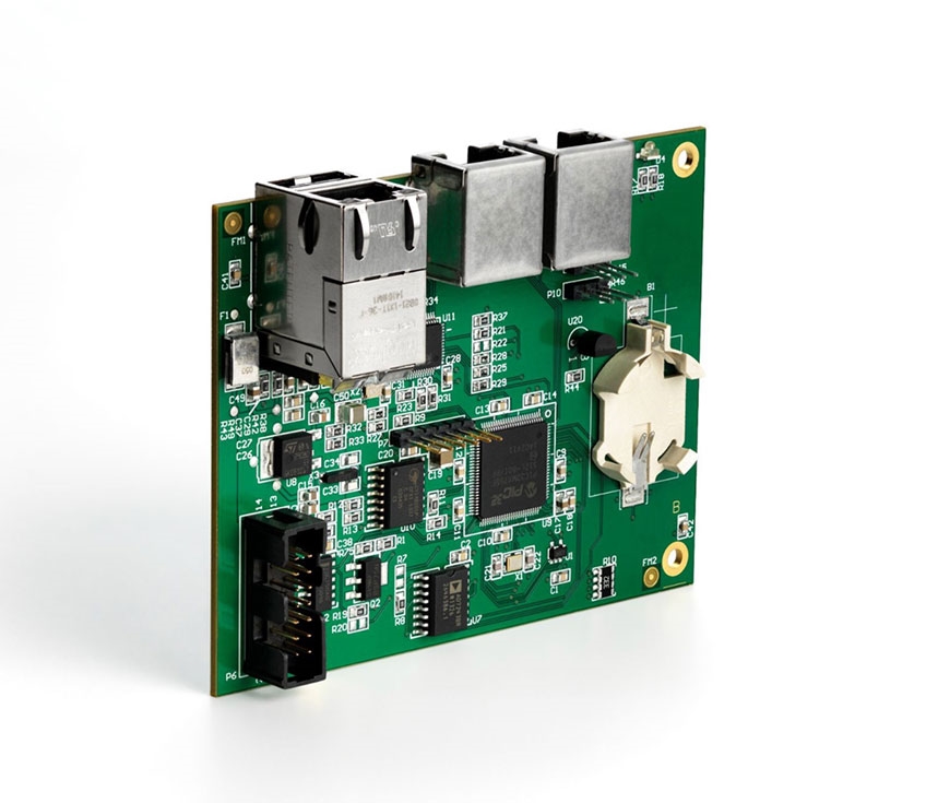
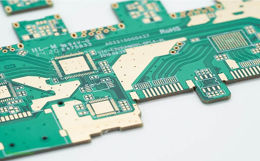
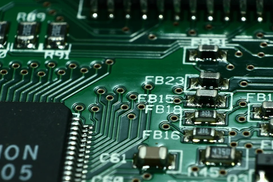
Multilayer FR4 PCB consists of multiple copper layers (typically 4-20+) laminated with epoxy resin (FR-4, Tg 130-180°C) and prepregs, enabling complex interconnections for high-density designs. Unlike single- or double-sided boards, they bury signals between planes for shielding, supporting via-in-pad for space savings and embedded components for slim profiles.
Why do they matter in 2025? With IoT devices exploding to 75 billion connections, per Statista forecasts, multilayer PCBs deliver the density needed for 10 Gbps speeds without ballooning footprints. In manufacturing, FR-4's affordability ($1-3/sq in at volume) and machinability make it ideal for high-density PCBs, but challenges like warpage during lamination (controlled to <0.75% per IPC-6012, Note 2) can derail runs. From factory perspectives, a solid FR-4 stackup ensures signal integrity by minimizing crosstalk < -50 dB, while power distribution planes cut voltage droop <5% on 1.8V rails. They're versatile for applications—from automotive ECUs enduring 125°C to consumer wearables prioritizing lightness. In essence, multilayer FR-4 bridges innovation and production, enabling reliable, scalable electronics that drive our connected world.
Technical Details of Multilayer FR-4 PCB Mechanisms
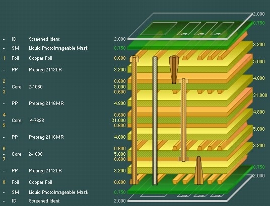
At their core, multilayer FR-4 PCBs rely on sequential lamination: Cores (0.8-1.6 mm FR-4 sheets) sandwich prepregs (0.1-0.2 mm resin-impregnated glass), pressed at 180-200°C/200-300 psi to fuse layers. Copper etching forms traces (4-6 mil widths), with vias (0.2-0.3 mm drills) plated for transitions. Let's break down key elements, drawing from production insights.
FR-4 Stackup Fundamentals
A typical 6-layer stackup alternates signals (L1/L3/L5) with planes (L2 GND/L4 PWR/L6 GND), using 1 oz Cu (35 µm) for low resistance <0.5 mΩ/sq. Dielectric thickness (5 mil prepreg) controls impedance—50 Ω microstrips via Z = 87 / √(ε_r +1.41) * ln(5.98h/(0.8w + t)) (IPC-2221B, Note 3).
Manufacturing Angle: Asymmetric stacks warp due to CTE differentials (FR-4 14 ppm/°C); factories mirror layers for symmetry, verified by IPC-TM-650 2.4.39 bow/warpage tests (Note 4). In high-density PCBs, thinner stacks (0.8 mm total) pack more, but demand precise alignment <0.1 mm.
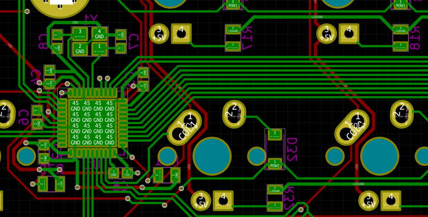
PCB Routing and Via Design Dynamics
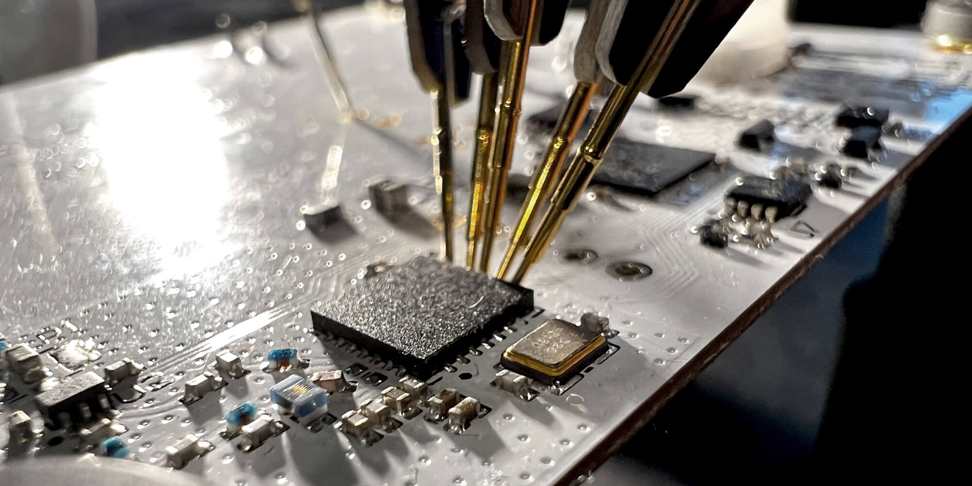
Routing weaves traces (min 4 mil/4 mil space) across layers, with vias bridging—through-hole for cost, blind/buried for density (aspect <8:1 per IPC-6012). Via design includes annular rings (0.15 mm) to prevent stubs reflecting at >5 GHz.
Details: Laser-drilled microvias (0.075 mm) in HDI PCB enable stacked vias, but plating voids >5% cause opens. Factories use sequential build-up (SBU) lamination to fill vias with electroplated Cu (15-20 µm), ensuring <1 nH inductance.
Signal Integrity and Power Distribution Mechanisms
Signal integrity combats losses: Crosstalk from parallel traces decays as e^(-d/h), where d=spacing, h=height. Power distribution networks (PDNs) use planes for <0.1 Ω up to 1 GHz, with decaps (0.1 µF) every 10 mm to damp transients.
Production Realities: In multilayer, plane splits radiate EMI; stitching vias (0.5 mm grid) contain fields. For high-density, simulations predict eye openings >200 mV at 10 Gbps, per JEDEC JESD79 (Note 5).
These layers interdepend: Poor via design disrupts routing, degrading integrity.
| Element | Key Parameter | Manufacturing Tolerance | Standard Reference |
|---|---|---|---|
| Stackup | 5 mil prepreg | ±0.05 mm thickness | IPC-4101C (Note 1) |
| Routing | 4 mil trace/space | ±0.02 mm etch | IPC-2221B (Note 3) |
| Via Design | 0.2 mm drill | Aspect <8:1 | IPC-6012 (Note 2) |
| Signal Integrity | Crosstalk < -50 dB | Spacing 3h min | JEDEC JESD79 (Note 5) |
| Power Distribution | <0.1 Ω plane | Stitch grid 0.5 mm | IPC-TM-650 (Note 4) |
This table summarizes critical specs.
Practical Solutions and Best Practices for Multilayer FR-4 PCBs
Factories thrive on proactive design-for-manufacturability (DFM). Here's a step-by-step approach, aligned with ISO 9001:2015 traceability (Note 6), to design, manufacture, and apply these boards effectively.
1. Crafting Optimal FR-4 Stackups
Start symmetric: L1 signal/L2 GND/L3 signal/L4 PWR for balanced CTE.
Steps:
- Simulation First: Use Polar SI9000 for impedance; target 50 Ω ±10%.
- Material Selection: High-Tg FR-4 (170°C) for reflow; 1080 prepreg for thinness.
- Lamination Controls: 190°C ramp, 2h dwell; measure warpage post-cool.
In practice, this prevents 90% delam issues in 8-layer runs.
2. Effective PCB Routing and Via Design
Route high-speed on inner layers; use blind vias for density.
Best Practices:
- Routing Rules: 45° bends; length-match diffs <25 ps.
- Via Optimization: Back-drill stubs >5 mm; electroless plating for 20 µm fill.
- DFM Check: Panelize with tabs; E-test 100% nets.
Factories report 25% shorter cycles with auto-routers tuned to these.
3. Safeguarding Signal Integrity
Adjacent planes shield signals; guard rings isolate analog.
Flow:
- Pre-Prod Sims: HyperLynx for < -60 dB isolation.
- Manufacturing Tweaks: Plasma desmear pre-drill; X-ray voids <3%.
- Applications Tip: For 5G, embed filters; test BER <10^-12.
4. Robust Power Distribution
Flood planes >90% coverage; decap grids for transients.
Practices:
- Plane Splits: Fence with 0.2 mm moats; stitch every λ/20.
- Thermal Management: Vias under ICs for <20°C rise.
- High-Density Focus: Microvia PDN for <0.05 Ω at 500 MHz.
5. Scaling for Applications
From automotive (AEC-Q100 qual, Note 7) to consumer: Use HDI for wearables.
Insight: Sustainable FR-4 (halogen-free) cuts e-waste 15% in 2025 eco-runs.
Case Study: Manufacturing 10-Layer FR-4 PCBs for a 5G Router
In Q3 2025, a telecom client grappled with 11% crosstalk fails in 10-layer prototypes (1.6 mm, RO4003C hybrid), where via stubs skewed signals 50 ps.
Challenges: Asymmetric stackup warped 0.9%; power droop hit 7% on 3.3V.
Solutions: Redesigned symmetric FR-4 stackup (5 mil prepregs); blind vias reduced stubs 60%. Routed diffs perpendicular, stitched planes every 3 mm. Lamination at 200 psi with IPC-TM-650 warpage checks (Note 4); inline TDR verified 50 Ω ±5%.
Outcomes: Yields reached 99%; production hit 30,000 units/month. Signal integrity improved to < -55 dB, powering reliable 10 Gbps links. This factory pivot saved $150K in scrap—highlighting multilayer FR-4's scalability for high-density apps.
Conclusion
Multilayer FR-4 PCBs, with thoughtful stackups, routing, and integrity measures, unlock a world of compact, high-performing electronics—from sensors to routers. By weaving in via innovations and power strategies, manufacturers deliver boards that meet 2025's density demands while staying manufacturable and affordable.
From the factory floor, a DFM review is your best ally. For your next multilayer project, prototype a stackup sim—it's the path to production peace.
FAQs
Q1: What defines a good FR-4 stackup for multilayer PCBs?
A1: Symmetric layers (signal/plane alternation) with 5 mil prepregs ensure <0.75% warpage (IPC-6012, Note 2). Target 50 Ω impedance; high-Tg FR-4 (170°C) for reflow. Factories use this for 98% yields in 2025 high-density boards.
Q2: How does PCB routing impact multilayer FR-4 performance?
A2: 4 mil traces with 45° bends minimize reflections; perpendicular routing cuts crosstalk < -50 dB. Per IPC-2221B (Note 3), length-match diffs <25 ps—essential for signal integrity in 10 Gbps apps.
Q3: What via design best suits high-density multilayer PCBs?
A3: Blind/microvias (aspect <8:1, 0.075 mm) save space; back-drill stubs for low inductance <1 nH. IPC-6012 (Note 2) guides plating; boosts density 50% in wearables.
Q4: How to maintain signal integrity in multilayer FR-4 PCBs?
A4: Adjacent GND planes and stitching (0.5 mm grid) shield < -60 dB; sim with HyperLynx for eye >200 mV. JEDEC JESD79 (Note 5) ensures BER <10^-12 in production.
Q5: What role does power distribution play in multilayer PCBs?
A5: Planes <0.1 Ω with decaps every 10 mm damp droops <5%; fence splits to curb EMI. IPC-TM-650 (Note 4) verifies; critical for low-power IoT in 2025.
Q6: Why choose multilayer FR-4 for high-density applications?
A6: Affordable HDI (IPC-4101C, Note 1) packs 1,000+ components; symmetric stacks prevent warpage. Ideal for 5G routers, yielding 99% at scale.
References
(Note 1) IPC-4101C — Specification for Base Materials for Rigid and Multilayer Printed Boards. IPC, 2006.
(Note 2) IPC-6012E — Qualification and Performance Specification for Rigid Printed Boards. IPC, 2017.
(Note 3) IPC-2221B — Generic Standard on Printed Board Design. IPC, 2012.
(Note 4) IPC-TM-650 — Test Methods Manual. IPC, latest edition.
(Note 5) JEDEC JESD79-4 — DDR4 SDRAM Standard (adapted for signal integrity). JEDEC, 2012.
(Note 6) ISO 9001:2015 — Quality Management Systems — Requirements. International Organization for Standardization, 2015.
(Note 7) AEC-Q100 — Stress Test Qualification for Integrated Circuits. Automotive Electronics Council, Rev-H, 2014.