What Defines a 16-Layer PCB Stackup and Why is it Crucial?
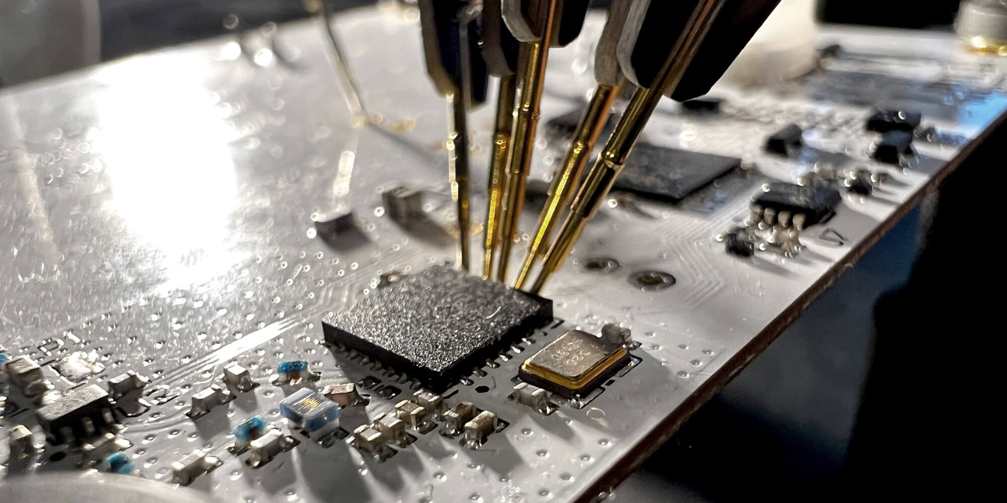
A 16-layer printed circuit board (PCB) stackup refers to the precise arrangement of sixteen alternating conductive copper and insulating dielectric layers. This intricate structure is engineered to support advanced electronic systems, incorporating layers dedicated to signal routing, robust ground planes for shielding, and stable power planes for voltage delivery. Such a complex build is fundamental for high-performance devices, including high-speed servers, sophisticated telecommunications gear, and cutting-edge medical equipment.
The thoughtful design of a 16-layer stackup profoundly influences several critical aspects of a PCB’s performance. Compared with other types of PCBs, it offers superior control over signal integrity by ensuring clean data transmission, facilitates consistent power delivery, aids in thermal management by dissipating heat, and is vital for controlling electromagnetic interference (EMI). A well-executed stackup allows for densely populated component layouts and protects high-speed signals from unwanted interference, thereby ensuring overall board reliability and efficiency.
What Are the Guiding Principles for a Robust 16-Layer PCB Design?
Crafting an effective 16-layer PCB stackup necessitates adherence to several core principles that collectively ensure optimal performance and manufacturability. These guidelines help in balancing intricate electrical requirements with practical production considerations.
Prioritizing Signal Integrity and EMI Control
For high-speed designs, maintaining signal integrity is paramount. This involves achieving controlled impedance—typically 50 ohms for single-ended signals and 100 ohms for differential pairs—by carefully positioning signal layers adjacent to stable reference planes (ground or power). Strategic distribution of ground planes also acts as a shield, significantly reducing noise and preventing interference between adjacent signal layers.
Optimizing Power Distribution and Manufacturability
Effective power distribution is achieved by placing power planes to minimize voltage drops and ensure a consistent current supply, often utilizing multiple planes for different voltage requirements (e.g., 3.3V, 5V). Furthermore, a balanced stackup contributes to even heat dissipation, preventing localized hotspots. Symmetrical layer arrangements are preferred to prevent board warping during fabrication, with appropriate dielectric thicknesses (e.g., 0.1 mm to 0.2 mm between layers) ensuring consistent electrical performance and ease of manufacturing.
What is a Recommended Layer Arrangement for a 16-Layer PCB?
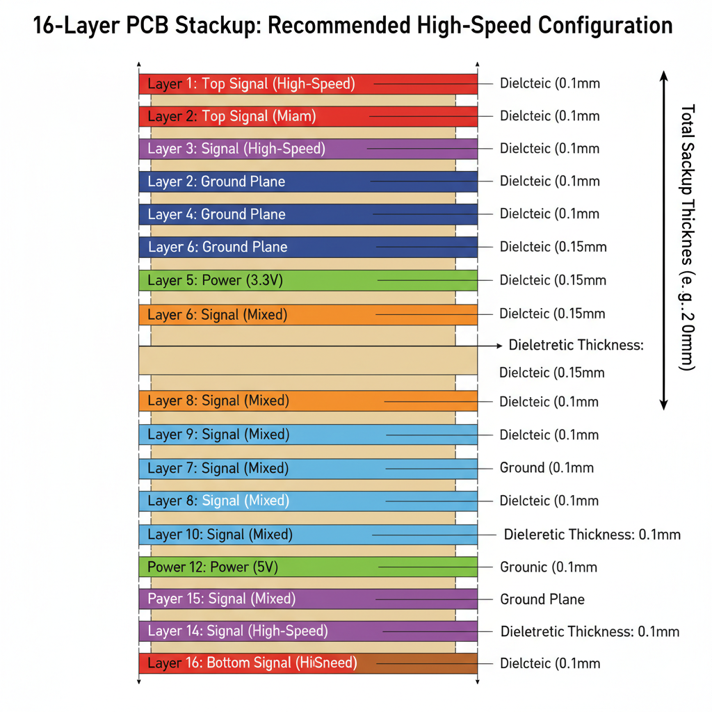
A common and effective configuration for a 16-layer PCB prioritizes placing critical signal layers near the outer surfaces for ease of routing, while internal layers are dedicated to stable power and ground planes. This structure helps in shielding and maintaining signal integrity for high-speed applications.
A highly practical arrangement for high-speed designs often follows this pattern, though it can be adapted based on specific project demands:
● Layer 1: Top Signal (Primary high-speed signals)
● Layer 2: Ground Plane
● Layer 3: Signal Layer (Secondary high-speed signals)
● Layer 4: Ground Plane
● Layer 5: Power Plane (e.g., 3.3V)
● Layer 6: Signal Layer (Mixed signals)
● Layer 7: Ground Plane
● Layer 8: Signal Layer (Mixed signals)
● Layer 9: Signal Layer (Mixed signals)
● Layer 10: Ground Plane
● Layer 11: Signal Layer (Mixed signals)
● Layer 12: Power Plane (e.g., 5V)
● Layer 13: Ground Plane
● Layer 14: Signal Layer (Tertiary high-speed signals)
● Layer 15: Ground Plane
● Layer 16: Bottom Signal (Critical high-speed signals)
This structure ensures that high-speed signal layers (1, 3, 14, 16) are closely coupled with ground planes, which is vital for controlled impedance and effective EMI shielding. Power planes are strategically placed internally to distribute voltage uniformly, while multiple ground planes serve to reduce noise and provide clear return paths for signals. The central layers (6, 8, 9, 11) offer flexibility for routing mixed or lower-speed signals, accommodating dense circuit layouts.
How Does Signal Layer Placement Impact 16-Layer PCB Performance?
The precise placement of signal layers is a cornerstone of maintaining optimal signal integrity, particularly in environments where data transfer rates frequently surpass 10 Gbps. Strategic positioning helps in managing impedance and minimizing unwanted noise.
Proximity to Reference Planes for Signal Integrity
High-speed signal layers should always be positioned immediately adjacent to a solid ground plane. This configuration, as demonstrated by Layers 1, 3, 14, and 16 in our recommended stackup, is crucial for minimizing loop inductance and ensuring a consistent return path for signals, thereby significantly reducing EMI. For instance, a 50-ohm trace on an outer layer can maintain its impedance with just 0.1 mm of dielectric separation from its underlying ground plane.
Isolating Different Signal Types and Routing Methods
It is essential to separate high-speed signals from slower analog or digital signals to prevent crosstalk. In the example stackup, the mid-range layers (6, 8, 9, 11) are designated for mixed or lower-speed signals, while the outer layers are reserved for mission-critical high-speed traces. Furthermore, outer signal layers (1 and 16) are optimally suited for microstrip routing (a signal path over a single ground plane), whereas internal signal layers (3 and 14) benefit from stripline routing (a signal path situated between two reference planes) for enhanced shielding and impedance control.
What is the Best Approach for Ground Plane Distribution to Reduce Noise?
Ground planes are foundational to a 16-layer PCB stackup, serving as critical low-impedance return paths for electrical signals and providing essential shielding against electromagnetic interference. Their effective distribution is key to a quiet, stable board.
Strategic Placement for Noise Reduction
To maximize noise reduction, ground planes must be placed in close proximity to signal layers. In the suggested stackup, ground layers (2, 4, 7, 10, 13, 15) are strategically interspersed among signal layers. This arrangement ensures that every active signal layer has an immediate reference plane, which is vital for maintaining stable impedance and mitigating noise.
Utilizing Multiple Ground Planes
A design incorporating six ground planes, as in the 16-layer example, offers opportunities to dedicate specific ground planes to different circuit sections, such as digital and analog grounds. This isolation prevents noise coupling between sensitive parts of the circuit. If a single unified ground is sufficient for the design, connecting all ground planes with numerous vias ensures a cohesive and robust reference plane across the entire board. It is generally advisable to avoid segmenting ground planes beneath active signal traces, as this can disrupt the signal return path and increase EMI. If splits are unavoidable in mixed-signal designs, care must be taken to ensure no signal traces cross these ground plane divisions.
How Should Power Planes Be Designed for Stable Voltage Delivery?
Power planes within a 16-layer PCB stackup are indispensable for supplying stable and consistent voltage to components, especially in designs that require multiple distinct voltage levels. Thoughtful design and positioning of these planes are crucial for overall system reliability.
Allocating Dedicated Voltage Layers
It is highly effective to dedicate specific internal layers to different voltage requirements. For instance, in our sample stackup, Layer 5 is allocated for 3.3V, and Layer 12 handles 5V. Should the design require additional voltages (e.g., 1.8V), another internal layer can be utilized, or an existing power plane can be carefully partitioned, provided this is done with meticulous planning to avoid current distribution issues.
Enhancing Stability Through Proximity and Decoupling
Placing power planes in close proximity to ground planes (e.g., Layer 5 adjacent to Layer 4) inherently creates a beneficial capacitance. This intrinsic capacitance acts as a distributed decoupling mechanism, effectively reducing noise and stabilizing voltage levels across the board. Employing a thin dielectric material (e.g., 0.05 mm) between these power and ground planes can further enhance this capacitive effect. Additionally, placing decoupling capacitors as close as possible to the power pins of integrated circuits, connected with short vias to both power and ground planes, is critical for mitigating voltage fluctuations during high-frequency switching operations. Similar to ground planes, minimizing splits in power planes is important to ensure uniform current distribution.
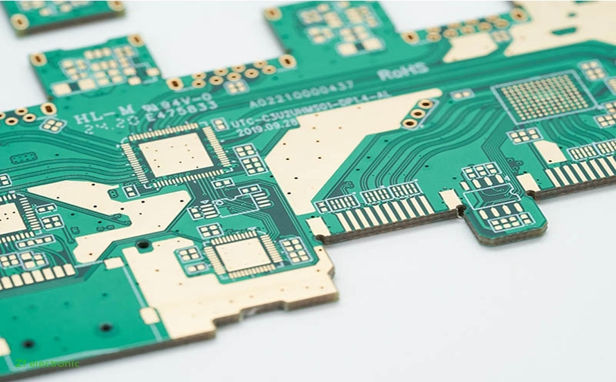
What are Key Considerations for Dielectric Materials and Thickness in 16-Layer PCBs?
The choice of dielectric material and its thickness between layers in a 16-layer PCB stackup profoundly influences signal impedance, propagation speed, and the overall manufacturability of the board. These factors are critical for achieving desired electrical performance.
Material Selection Based on Application Needs
For standard designs, common materials like PCB FR-4, with a dielectric constant ranging from 4.2 to 4.5, offer a cost-effective solution. However, for high-speed applications where signal attenuation is a concern, low-loss materials such as Rogers 4350B, possessing a dielectric constant of 3.48, are often preferred. The selection of the material should align directly with the operational frequency and performance targets of the circuit.
Dielectric Thickness for Impedance Control and Symmetry
Maintaining a consistent dielectric thickness between signal layers and their respective reference planes is vital for achieving controlled impedance (e.g., 0.1 mm for 50-ohm traces). Thicker dielectrics, such as 0.2 mm, may be used between power and ground planes to increase capacitance. Furthermore, ensuring a symmetrical stackup, where the top half of the board closely mirrors the bottom half in terms of layer order and thickness, is crucial to prevent warping during the fabrication process.