Why Opt for a 10-Layer PCB Stackup in High-Speed Designs?
A 10-layer PCB stackup strikes an optimal balance between intricacy and utility for advanced electronic systems. With numerous layers strategically designated for signals, power, and ground planes, this configuration provides the necessary adaptability to manage high-speed signals while significantly reducing interference. Unlike simpler 4 or 6-layer circuit boards, a 10-layer design facilitates superior separation of critical signals, enhanced power distribution, and improved electromagnetic compatibility (EMC).
High-speed designs frequently operate at frequencies where maintaining signal integrity becomes a considerable challenge. A meticulously engineered 10-layer stackup effectively addresses these issues by offering dedicated layers for controlled impedance traces and actively mitigating crosstalk between signals. Furthermore, the increased layer count supports denser routing, making it an ideal choice for compact devices populated with a high number of components.
Key Advantages of a 10-Layer Stackup
● Enhanced Signal Integrity: The inclusion of multiple ground planes effectively dampens noise and provides a robust, stable reference for high-speed signals.
● Precise Impedance Control: Dedicated layers enable consistent trace geometry, ensuring that impedance values align precisely with targets, such as 50Ω for single-ended signals or 90Ω for differential pairs.
● Superior Power Distribution: Separate power planes are instrumental in minimizing voltage drops and guaranteeing a stable, consistent power supply to all components.
● Reduced Electromagnetic Interference (EMI): A well-thought-out layer arrangement acts as a shield, protecting sensitive signals from external electromagnetic interference.
How to Design a 10-Layer PCB Stackup for Optimal Impedance Control
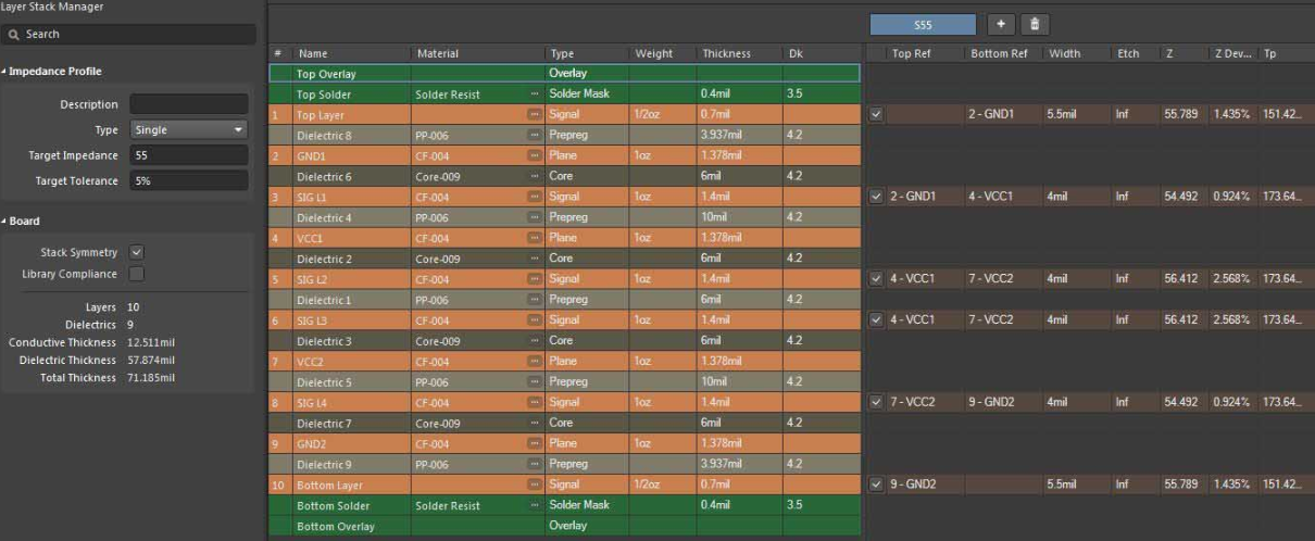
Impedance control is an indispensable element in high-speed PCB design, especially within a 10-layer stackup. Without correct impedance matching, signals can experience reflections, potentially leading to data corruption or loss. In a 10-layer PCB stackup, achieving precise impedance control begins with a meticulous arrangement of layers and careful attention to trace geometry, ensuring consistent electrical characteristics across the entire board.
For example, a common impedance target for high-speed digital signals is 50Ω for single-ended traces. Attaining this requires stringent control over factors such as trace width, spacing, and the dielectric thickness separating the trace from its reference plane. Within a 10-layer stackup, you can allocate specific layers for high-speed signals, positioning them immediately adjacent to ground planes to create an ideal controlled impedance environment.
Steps for Achieving Precise 10-Layer PCB Stackup Impedance Control
● Define Impedance Requirements: Clearly identify the precise impedance values needed for your specific design, such as 50Ω for single-ended traces or 100Ω for differential signals.
● Select Appropriate Materials: Utilize dielectric materials that exhibit a consistent dielectric constant (Dk) to prevent impedance variations. Typical values for the standard PCB FR-4 material range from 3.5 to 4.5.
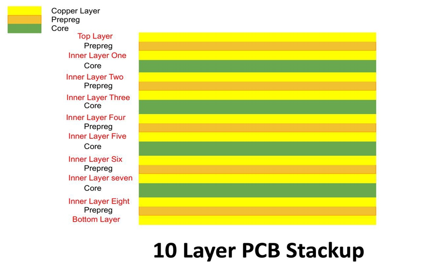
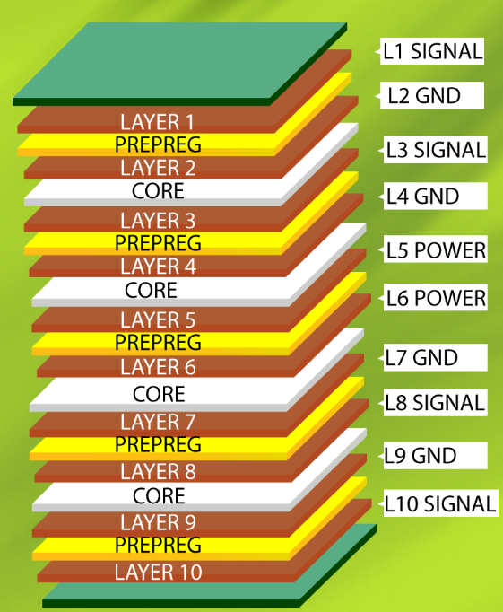
● Plan Layer Arrangement Strategically: Position signal layers directly next to ground planes to establish a stable reference and minimize loop inductance. A typical 10-layer configuration might involve signal layers on L1, L3, L8, and L10, with corresponding ground planes on L2, L4, L7, and L9.
● Calculate Trace Geometry Accurately: Employ an impedance calculator to determine the precise trace width and spacing, taking into account the dielectric thickness and material properties. For instance, on a 1.6mm thick board, a 50Ω trace might require a width of approximately 6-8 mils on the outer layers.
● Verify Through Simulation: Leverage field solver tools to simulate impedance characteristics and make necessary adjustments prior to board fabrication.
By diligently following these steps, you can ensure your 10-layer PCB stackup meets the rigorous impedance requirements of high-speed applications, effectively reducing signal reflections and guaranteeing reliable data transmission.
Ensuring Robust Signal Integrity in a 10-Layer PCB Stackup
Signal integrity measures how effectively an electrical signal maintains its intended shape and timing as it traverses the fast turn PCB. In high-speed designs, elements such as crosstalk, unwanted noise, and signal delays can severely degrade performance. A 10-layer PCB stackup offers distinct advantages for preserving signal integrity by providing ample room for comprehensive shielding and sophisticated routing optimization.
One of the primary techniques for ensuring strong 10-layer PCB stackup signal integrity involves the strategic use of multiple ground planes. These planes function as effective shields, significantly reducing crosstalk between adjacent signal layers and providing a low-impedance return path for high-speed signals. For example, inserting a ground plane between two signal layers can reduce crosstalk by as much as 20 dB compared to designs lacking such separation.
Strategies for Optimizing Signal Integrity
● Minimize Via Transitions: Every via introduces parasitic inductance and capacitance, which can cause signal reflections. Wherever feasible, route critical signals entirely on a single layer, or utilize back-drilling to eliminate unused via stubs.
● Implement Differential Pairs: For high-speed signals, route differential pairs with consistent spacing (e.g., 5 mils apart for 100Ω impedance) to maintain signal balance and common-mode noise rejection.
● Avoid Routing Over Splits: Crucially, ensure that high-speed traces do not cross over splits or gaps in power or ground planes, as this disrupts the essential return current path and significantly increases noise.
● Incorporate Decoupling Capacitors: Strategically place decoupling capacitors close to the power pins of high-speed components to stabilize voltage rails and effectively reduce switching noise. A common value for high-speed designs is 0.1 μF.
By meticulously planning your 10-layer PCB stackup with these principles in mind, you can achieve clean, dependable signals even at frequencies exceeding 1 GHz, making your design suitable for demanding applications like DDR4 memory interfaces or high-speed serial links.
Selecting the Right Materials for a 10-Layer PCB Stackup
Material selection plays a paramount role in the overall performance of a 10-layer PCB stackup, especially when designing for high-speed applications. The dielectric material situated between layers directly influences impedance characteristics, signal loss, and thermal stability. Simultaneously, the copper thickness impacts both current-carrying capacity and trace resistance. Choosing the correct 10-layer PCB stackup materials ensures that your board can effectively handle high frequencies and endure challenging operating conditions.
Key Material Selection Considerations
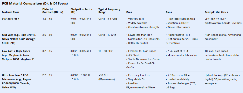
● Dielectric Constant (Dk): A lower Dk value (e.g., 3.0-3.5) is beneficial as it minimizes signal propagation delay and reduces loss, making materials like specialized high-frequency laminates an excellent choice for designs operating above 5 GHz. Standard FR-4, with a Dk of 4.2-4.5, remains suitable for lower-frequency applications.
● Dissipation Factor (Df): A lower Df (e.g., 0.002-0.005) is crucial for minimizing signal loss at high frequencies. High-performance materials typically offer a much lower Df compared to standard FR-4 (which has a Df of around 0.02) in this regard.
● Thermal Stability: Materials exhibiting a high glass transition temperature (Tg), ideally 170°C or higher, are essential to prevent delamination and warping during the soldering process and throughout operational life.
● Copper Weight: Utilizing 1 oz copper (approximately 35 μm) for signal layers provides a balanced approach between manufacturability and electrical performance. For power planes, employing 2 oz copper (approximately 70 μm) can effectively manage higher currents without excessive heat buildup.
For the majority of 10-layer PCB stackups, a hybrid material approach—combining standard FR-4 for less critical inner layers with high-frequency materials for the outer signal layers—often presents a cost-effective solution. This strategy ensures that critical high-speed signals benefit from low-loss materials while keeping overall manufacturing costs manageable.
Understanding Common 10-Layer PCB Stackup Configurations
While the precise arrangement of a 10-layer PCB stackup will naturally vary depending on the specific demands of your design, several established configurations prove highly effective for high-speed applications. These configurations strategically prioritize signal integrity, impedance control, and efficient power distribution by carefully positioning signal, ground, and power layers.
Illustrative Configuration for High-Speed Designs
|
Layer |
Type |
Primary Purpose |
|
L1 |
Signal |
Top layer, typically for high-speed signals |
|
L2 |
Ground |
Stable reference plane for L1 and L3 |
|
L3 |
Signal |
Inner signal layer, optimized for routing |
|
L4 |
Ground |
Shielding and additional reference plane |
|
L5 |
Power |
Primary power distribution plane |
|
L6 |
Power |
Secondary power distribution plane |
|
L7 |
Ground |
Reference plane for L6 and L8 |
|
L8 |
Signal |
Inner signal layer, optimized for routing |
|
L9 |
Ground |
Reference plane for L8 and L10 |
|
L10 |
Signal |
Bottom layer, also suitable for high-speed signals |
This specific configuration ensures that every signal layer is directly adjacent to a ground plane, thereby providing a stable reference for precise impedance control and substantially reducing crosstalk. Power planes are strategically situated in the central region of the stackup to minimize interference with signal layers while simultaneously ensuring highly efficient power delivery.
Addressing Challenges in 10-Layer PCB Stackup Design and Their Solutions
Designing a 10-layer PCB stackup for peak high-speed performance naturally presents its own set of complexities. From effective thermal management to ensuring manufacturability, engineers must skillfully navigate various factors to produce a reliable circuit board.
Common Design Challenges
● Thermal Management: High-speed components invariably generate significant heat, which can lead to issues such as warping or delamination in a multi-layer board.
● Manufacturing Tolerances: Even minor variations in dielectric thickness or trace width can adversely affect impedance, a particularly sensitive issue in high-frequency designs.
● Cost Implications: The use of advanced materials and the inherent complexity of multi-layer stackups often increase fabrication costs, which may not be viable for every project budget.
Practical Solutions and Strategies
● Employ Thermal Vias: Integrate thermal vias strategically near heat-generating components to efficiently transfer heat to internal layers or external heatsinks.
● Engage Fabricators Early: Establish close collaboration with your manufacturing partner at an early stage to define achievable tolerances and adjust your design accordingly.
● Optimize Material Selection: Balance the trade-offs between performance and cost by selectively using high-performance materials only where absolutely critical, such as for outer signal layers.
By anticipating these challenges and proactively implementing targeted solutions, you can create a 10-layer PCB stackup that consistently performs reliably without exceeding predetermined budget constraints.
Conclusion: Achieving High-Speed Success Through 10-Layer PCB Stackup Mastery
A meticulously designed 10-layer PCB stackup serves as an exceptionally powerful tool for attaining superior high-speed performance in contemporary electronics. By rigorously concentrating on impedance control, ensuring robust signal integrity, and making judicious material selections, you can engineer a circuit board that effectively meets the stringent demands of even the most intricate applications. Whether you are routing high-speed signals for a sophisticated data center or developing a compact device with extremely tight spacing, the principles thoroughly outlined in this guide will empower you to unleash the full potential of your 10-layer PCB stackup.
From the careful arrangement of layers to the informed selection of appropriate materials, every decision made throughout the design process profoundly impacts the ultimate performance of your board. Dedicate ample time to simulate, thoroughly test, and meticulously refine your stackup; this diligent effort will be rewarded with a design that delivers pristine signals, stable power, and enduring reliability. Armed with these insights, you are exceptionally well-prepared to successfully navigate the complexities of high-speed PCB design and transform your innovative concepts into tangible reality.