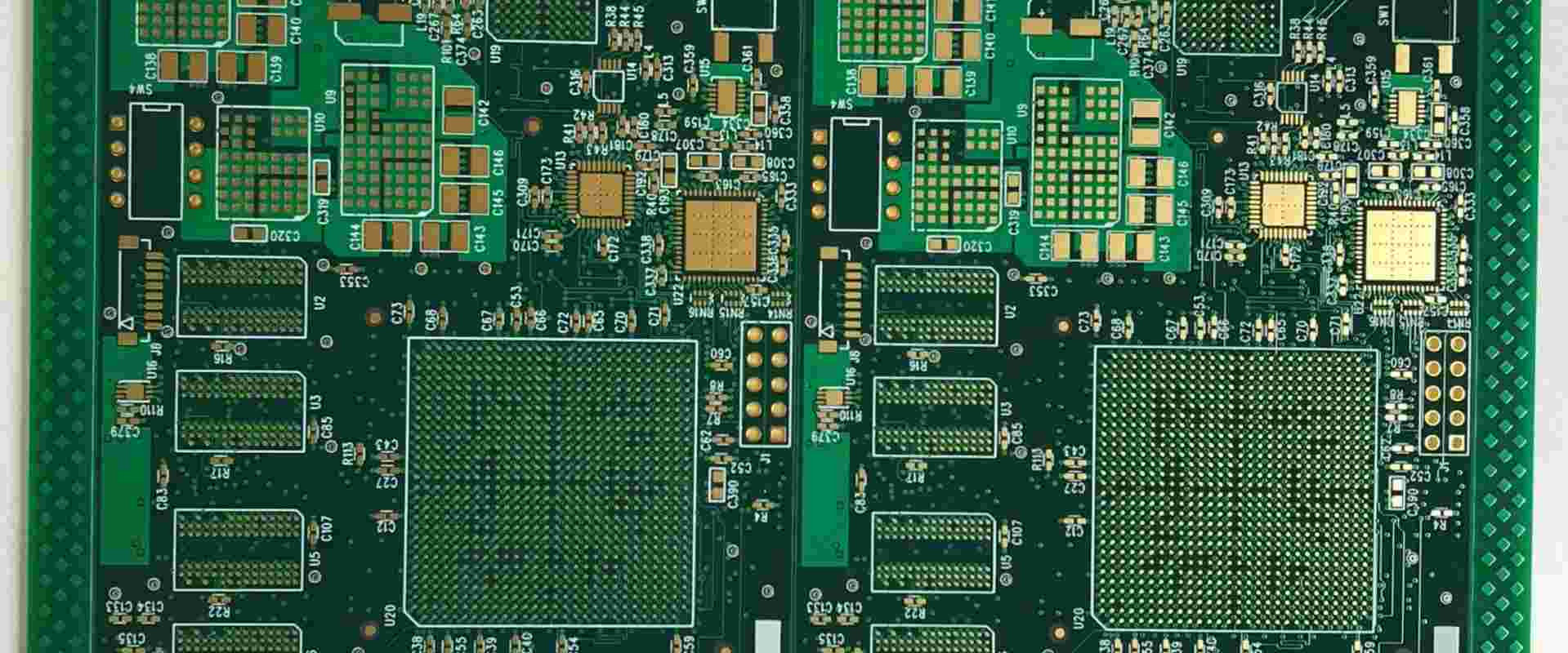
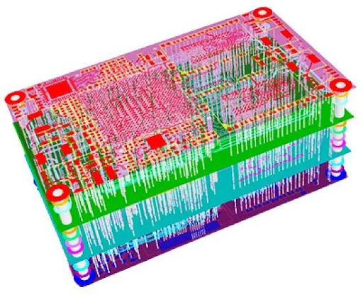
What Defines a 12-Layer PCB Stackup and Its High-Speed Advantages?
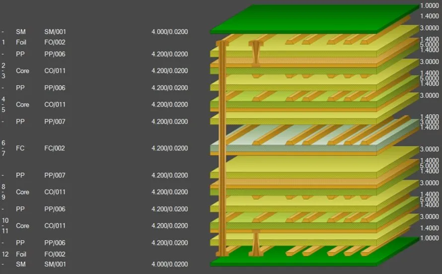
A 12-layer PCB stackup refers to the precise arrangement of twelve alternating layers of conductive copper and insulating dielectric materials within a Printed Circuit Board. This intricate structure is specifically engineered to manage multiple functionalities, including signal routing, power distribution, and grounding, which are critical for high-speed and high-frequency applications like telecommunications, advanced computing, and data center infrastructure.
In designs where signals operate above 100 MHz, challenges such as crosstalk, electromagnetic interference (EMI), and signal loss become significant. A 12-layer configuration offers sufficient layers to effectively isolate high-speed signals, dedicate robust planes for power and ground, and precisely control impedance. This layered approach helps to drastically minimize noise and ensures dependable performance, making it an optimal choice for complex and performance-intensive circuits.
Benefits of a Multi-Layer Stackup for Advanced Electronics
The principal advantages of a 12-layer PCB stackup lie in its ability to significantly enhance crucial performance metrics. It provides superior signal integrity by allowing dedicated signal routing layers and effective shielding, which drastically reduces interference. The structure also ensures improved power distribution through separate, continuous power and ground planes, leading to stable voltage delivery across the board. Furthermore, precise layer arrangement is instrumental in achieving stringent impedance control, essential for maintaining consistent signal characteristics for high-speed data transmission. This dense layering also facilitates a compact design, packing more circuitry into a smaller physical footprint—a vital requirement for modern, miniaturized electronic devices.
Achieving Precise Impedance Control in 12-Layer PCB Stackups
Impedance control is a foundational element in high-speed PCB design, dictating how a signal propagates through a trace. In a 12-layer PCB stackup, impedance is influenced by trace width, dielectric thickness, and material properties. Deviations from target impedance can cause signal reflections, leading to data errors and degraded system performance.
Strategic Layering for Stable Impedance
To ensure effective 12-layer PCB stackup impedance control, designers must meticulously plan the arrangement of layers and carefully select materials. For instance, single-ended high-speed traces typically require a characteristic impedance of 50 ohms, while differential pairs often target 100 ohms. Critical to this is layer symmetry, where signal layers are arranged symmetrically around the board's center. This balances mechanical stresses and helps maintain consistent electrical properties. Reference planes are equally important, with high-speed signal layers placed directly adjacent to continuous ground or power planes to provide a stable return path and consistent reference. Finally, precise trace geometry is determined using impedance calculators that factor in the dielectric constant (Dk) of the material (often 3.5 to 4.5 for standard FR-4), trace width, and the distance to the reference plane. For example, a 50-ohm trace on layer 2 might be referenced to a ground plane on layer 3, separated by approximately 0.1 mm of dielectric material. Specialized tools like field solvers integrated into PCB design software are invaluable for simulating and verifying these impedance values prior to fabrication.
Optimizing 12-Layer PCB Stackup for Signal Integrity
Signal integrity (SI) is paramount; it's the measure of a signal's ability to retain its intended shape and timing as it travels across the PCB. Compromised SI can result in data corruption, timing inaccuracies, and system malfunctions. A thoughtfully engineered 12-layer PCB stackup for signal integrity actively mitigates these issues by minimizing noise and interference.
Best Practices for Robust Signal Paths
To achieve optimal signal integrity in a 12-layer stackup, several best practices are employed. Dedicated signal layers, particularly inner layers (e.g., layers 2, 4, 9, 11), are reserved for high-speed signals, providing inherent shielding from external noise sources. Maintaining ground plane proximity is crucial, as placing high-speed signals very close to a continuous ground plane reduces loop inductance and electromagnetic interference (EMI). To minimize crosstalk, critical signals should be routed on separate layers or with ample spacing (e.g., at least three times the trace width) to prevent unwanted capacitive or inductive coupling. Finally, careful via management, including techniques like back-drilling or the use of blind vias, is essential to reduce "stub effects" that can significantly degrade signal quality at frequencies exceeding 1 GHz. In a typical 12-layer configuration, outer layers (1 and 12) might handle low-speed signals or components, while inner layers (2 and 11) are dedicated to high-speed signals. Layers 3, 5, 8, and 10 could function as solid ground planes, effectively sandwiching and shielding the high-speed signals. This arrangement ensures clean signal paths and effectively manages EMI.
Material Selection for High-Performance 12-Layer Stackups
The choice of materials directly influences a PCB's electrical and thermal performance, especially critical for high-speed designs. When selecting 12-layer PCB stackup materials, key considerations include dielectric constant (Dk), loss tangent (Df), thermal stability, and cost-effectiveness.
Common and Advanced Laminates
For standard applications up to 1 GHz, FR4 PCB remains a cost-effective choice with a Dk typically between 4.2–4.5. However, its higher loss tangent means increased signal attenuation at higher frequencies. For designs exceeding 1 GHz, high-speed laminates like Isola 370HR or Rogers 4350B are preferred. These materials offer lower Dk values (around 3.0–3.5) and significantly lower loss tangents (0.003–0.009), ensuring minimal signal loss. It's essential to use compatible prepreg (resin-impregnated glass fabric) and core materials to maintain consistent dielectric properties throughout the stackup. For a balanced approach, a hybrid stackup might combine cost-effective FR-4 for power and ground planes with specialized high-speed laminates for critical signal layers. Additionally, designers must ensure that the material’s Coefficient of Thermal Expansion (CTE) is matched across layers to prevent board warpage during fabrication and operation.
Essential Design Rules for 12-Layer PCB Stackups
Adhering to stringent 12-layer PCB stackup design rules is crucial for successful manufacturing and ensures the board meets its performance specifications. These guidelines govern layer organization, spacing, and routing practices, particularly for high-speed applications.
Critical Rules for Robust Stackup Design
A fundamental rule is maintaining a symmetrical stackup in terms of layer thickness and material composition. This prevents undesirable board warpage during manufacturing and thermal cycling. For example, if the top layer (L1) is a signal layer, the bottom layer (L12) should ideally mirror its characteristics. Dedicated power and ground planes are essential; at least two layers for each (e.g., L6 and L7 centrally placed) ensure low impedance power delivery paths and effective decoupling. Dielectric thickness between signal and reference layers must be kept consistent (e.g., 0.1–0.2 mm) to precisely control impedance.
In routing guidelines, avoid routing high-speed signals across split planes, as this discontinuity disrupts the signal return path and generates EMI. For via placement, minimize the number of via transitions for high-speed signals. When vias are necessary, place adjacent ground vias to provide a clear and low-inductance return path, which helps mitigate signal degradation. Early consultation with your PCB fabrication partner is highly recommended to confirm their manufacturing capabilities and specific design constraints, ensuring manufacturability and cost-effectiveness.
Cost Analysis for 12-Layer PCB Stackups
While 12-layer PCB stackups offer superior performance for complex designs, their increased layer count inherently translates to higher PCB cost. Understanding the key cost drivers is essential for making informed design decisions without compromising quality.
Factors Influencing 12-Layer PCB Fabrication Costs
Several elements contribute to the overall 12-layer PCB stackup cost. The material selection is a significant factor; high-speed laminates are considerably more expensive than standard FR-4. Strategic use of advanced materials only for critical signal layers can help manage costs. The layer count itself directly increases cost due to additional processing steps like lamination, drilling, and plating compared to boards with fewer layers. Manufacturing complexity also drives costs up; features such as blind or buried vias, extremely tight tolerances, or very thin dielectric layers demand more advanced fabrication techniques. Production volume plays a role, with higher volumes typically yielding lower per-unit costs, while small-batch orders incur higher per-unit expenses due to fixed setup costs. Finally, specialized testing requirements, such as comprehensive impedance testing or advanced quality assurance checks, add to the overall expenditure but are crucial for ensuring reliability in high-speed applications. To optimize costs, designers should explore using standard materials where high-speed performance isn't critical and simplify the design where possible by reducing the variety of via types or layer transitions. Close collaboration with the manufacturing partner can often reveal further cost-saving opportunities without sacrificing essential performance.
Practical Strategies for Designing a 12-Layer PCB Stackup
Designing a 12-layer PCB stackup for high-speed applications can be intricate, but adopting a structured approach can significantly streamline the process and improve design outcomes.
Key Tips for a Successful High-Speed Stackup
Begin the design process with comprehensive simulation. Utilize advanced PCB design software to model and analyze impedance characteristics, signal integrity, and potential electromagnetic interference (EMI) issues before finalizing the stackup. This proactive step can identify and resolve problems early, saving considerable time and expense. Establish early collaboration with your PCB fabrication team; engaging them during the design phase is crucial to align on material availability, specific manufacturing capabilities, and any potential constraints, ensuring the design is manufacturable. Prioritize critical signals by allocating the best-shielded inner layers to the fastest and most sensitive signals, reserving the less protected outer layers for lower-speed or less critical traces. Finally, meticulous documentation is key. Maintain detailed records of all layer functions, impedance targets, material specifications, and any design decisions. This documentation serves as an invaluable resource for future reference, debugging, and potential design iterations. By implementing these strategies, designers can effectively navigate the complexities of 12-layer stackup design and achieve both technical performance goals and budgetary objectives.
Conclusion: Achieving High-Speed Success with 12-Layer PCB Stackups
Designing a 12-layer PCB stackup for high-speed applications is a sophisticated process that requires a careful balance of performance, complexity, and cost considerations. By rigorously focusing on 12-layer PCB stackup impedance control, ensuring robust signal integrity, judiciously selecting materials, strictly adhering to established design rules, and strategically managing costs, engineers can develop highly reliable and high-performance boards for even the most demanding electronic projects.
This guide has provided a comprehensive overview of the critical aspects involved in 12-layer stackup design, from understanding its fundamental structure to applying advanced best practices. Equipped with this specialized knowledge, you are now better prepared to navigate the intricate challenges inherent in high-speed PCB design and deliver cutting-edge solutions. Continuous iteration, rigorous testing, and a commitment to refining your approach will be essential to staying at the forefront of the rapidly evolving world of electronics design.