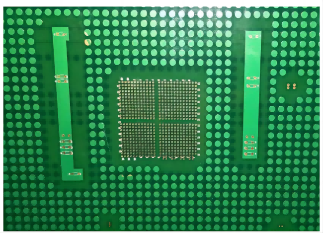
Introduction
Warpage remains one of the most frequent reject causes in high-layer-count and large-panel multilayer PCBs. Excessive bow and twist directly affect SMT yield, BGA coplanarity, and long-term reliability in automotive, server, and aerospace applications. Modern designs with 20–40 layers, asymmetric stackups, thin cores, and heavy copper push warpage limits further. This article examines the fundamental PCB warpage causes during lamination and post-processing, and details proven factory-level prevention and stress relief techniques that consistently achieve <0.5% warpage on complex boards.
Primary PCB Warpage Causes in Multilayer Manufacturing
1. Copper Distribution Imbalance
The single largest contributor. Residual stress develops when copper loading differs by more than 10% between symmetric layers after etching.
2. CTE Mismatch in the Z-Axis
Copper CTE ≈ 17 ppm/°C Resin system CTE below Tg ≈ 50–70 ppm/°C, above Tg ≈ 200–300 ppm/°C This mismatch creates tensile stress during cooling from 180 °C lamination temperature.
3. Asymmetric Resin Distribution
Large copper-free areas fill with excess prepreg resin, leading to localized shrinkage differences.
4. Lamination Cycle Asymmetry
Uneven heating/cooling rates, unbalanced pressure, or missing separator plates generate built-in stress.
5. Post-Lamination Processing
Solder mask curing, ENIG plating, and sequential lamination cycles add additional asymmetric thermal loads.
Material Selection Anti-Warpage Strategies
| Material Choice | Warpage Impact | Typical Application |
|---|---|---|
| Low-CTE cores (≤30 ppm/°C) | Significantly reduces Z-axis expansion | >20-layer backplanes |
| High-Tg (≥170 °C) resin systems | Lowers stress release above Tg | Lead-free assembly boards |
| Spread-glass or no-glass reinforcement | Eliminates glass-stop effect, improves symmetry | RF + digital hybrid boards |
| Symmetrical prepreg types | Balances resin content top/bottom resin flow | All high-layer-count designs |
Lamination Process Controls That Prevent Warpage
- Symmetrical Book Construction: Mirror-image panel pairing in every book. Never press odd number of panels.
- Slow Controlled Cooling: Cool from 130 °C to 80 °C at ≤2 °C/min under full pressure. Fast cooling locks in stress.
- Caul Plate and Cushion Management: Use 1.5 mm polished stainless caul plates with fresh kraft paper or silicone rubber cushions on both sides.
- Pressure Profile Optimization: Apply full pressure only after resin gels (>120 °C). Early high pressure squeezes resin asymmetrically.
- Post-Lamination Stress Relief Baking: Bake panels at 150 °C for 4–6 hours immediately after press unloading while still clamped between flat plates.
Design-Level Warpage Prevention Techniques
| Technique | Implementation Detail | Typical Warpage Reduction |
|---|---|---|
| Copper balancing | Keep copper % within ±5% between mirrored layers | 40–60% |
| Dummy copper thieving | Add hatched or solid copper in sparse areas | 30–50% |
| Core thickness symmetry | Pair 0.1 mm core with another 0.1 mm core | Essential |
| Prepreg symmetry | Identical 1080 × 4 top and bottom | 20–30% |
| Panel border copper frame | 10–15 mm wide solid copper ring around panel | 15–25% |
Post-Lamination Stress Relief Techniques
- Hot Clamp Baking: Place panels between two thick aluminum plates and bake 150 °C / 6 hours with light clamping force.
- Vacuum Stress Relief: Vacuum bag panels with breather cloth at 160 °C / 4 hours. Removes moisture and relaxes resin stress.
- Sequential Lamination Warpage Correction: After first lamination, measure warpage direction. Adjust next layup to counter-bow (add more prepreg on concave side).
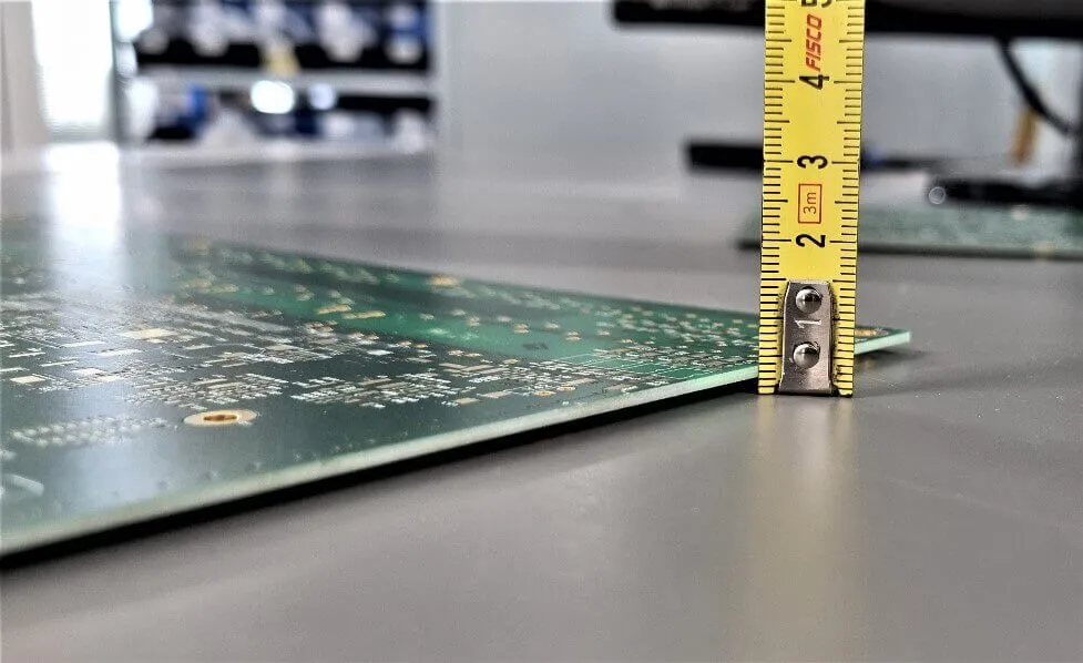
Measurement and Acceptance Criteria
- IPC-TM-650 2.4.22C — Bow and Twist on bare panels
- IPC-6012E Section 3.4.3 — Maximum 0.75% for SMT boards, 1.5% for non-SMT
- For >500 mm panels, many OEMs tighten to ≤0.5%
Real Factory Results After Implementing Full Anti-Warpage Flow
| Board Type | Layers | Size (mm) | Before Optimization | After Optimization |
|---|---|---|---|---|
| Server motherboard | 24 | 550×650 | 1.2–2.1% | 0.3–0.5% |
| 5G AAU digital board | 18 | 420×380 | 0.9–1.6% | 0.2–0.4% |
| Automotive radar hybrid | 10 | 120×160 | 1.1–1.8% | <0.3% |
Conclusion
Warpage in multilayer PCBs is not inevitable. It is a predictable result of copper imbalance, CTE mismatch, and uncontrolled thermal history. By enforcing strict copper symmetry, selecting low-CTE and high-Tg materials, applying slow cooling under pressure, and performing immediate post-lamination stress relief baking, manufacturers routinely achieve <0.5% warpage even on 30+ layer, 600 mm panels. These factory-proven controls eliminate the most common and costly defect in advanced fast turn circuit board manufacturing.
FAQs
Q1: What is the single biggest cause of PCB warpage in multilayer manufacturing? Asymmetric copper distribution between mirrored layers. Differences >10% almost always produce visible bow after lamination.
Q2: Does slower cooling really reduce warpage that much? Yes. Cooling at ≤2 °C/min from 130 °C to 80 °C under pressure can reduce warpage by 50–70% compared to natural cooling.
Q3: Can material selection alone prevent warpage? No. Low-CTE cores help, but without copper balancing and proper lamination control, warpage will still exceed 1%.
Q4: When should I perform stress relief baking? Immediately after lamination while panels are still hot, or within 4 hours maximum. Delayed baking is far less effective.
References
IPC-6012E — Qualification and Performance Specification for Rigid Printed Boards. IPC, 2020.
IPC-TM-650 2.4.22C — Bow and Twist Determination. IPC, 2018.
IPC-4101E — Specification for Base Materials for Rigid and Multilayer Printed Boards. IPC, 2017.
IPC-A-600K — Acceptability of Printed Boards. IPC, 2020.