Introduction
The physical arrangement of copper layers and dielectrics in a multi-layer PCB determines signal integrity, power integrity, and EMC performance more than any other single factor. A well-optimized multi-layer PCB stackup provides low-inductance power distribution, continuous return paths, controlled characteristic impedance, and inherent noise shielding. This guide presents industry-proven stack-up strategies that achieve excellent signal integrity and power distribution from 4 layers to 16 layers.
Fundamental Principles of Good Stackups
- Every routing layer must be adjacent to at least one solid reference plane (GND or PWR)
- High-speed signals require the closest possible spacing to their return plane (≤ 0.15 mm preferred)
- Power and ground planes should be paired tightly (≤ 0.10 mm) to create high-frequency decoupling capacitance
- Maintain symmetry about the center to minimize warpage
- Use thin dielectrics (0.076–0.15 mm prepreg) between critical layer pairs
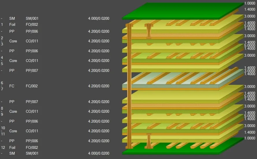
Recommended Stackups by Layer Count
4-Layer (Best Beginner Choice)
- L1: Signal (horizontal)
- L2: Ground (solid)
- L3: Power (can be split carefully)
- L4: Signal (vertical)
- Core: 1.0–1.2 mm, Prepreg: 0.15–0.20 mm
- Spacing L1-GND and PWR-L4 ≈ 0.18 mm gives ~50–60 Ω single-ended impedance.
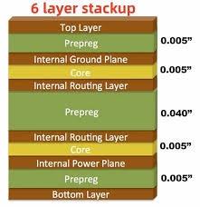
6-Layer (Most Popular for Mixed-Signal)
- L1: Signal (horizontal)
- L2: Ground
- L3: Signal (vertical)
- L4: Power
- L5: Ground
- L6: Signal (horizontal)
- All routing layers are sandwiched between planes. L2-L5 spacing ≤ 0.15 mm creates excellent interplane capacitance.
8-Layer (High-Speed Standard)
- L1: Signal (horizontal)
- L2: Ground
- L3: Signal (vertical)
- L4: Power
- L5: Power
- L6: Ground
- L7: Signal (vertical)
- L8: Signal (horizontal)
- Provides two dedicated routing pairs with perfect reference planes and thick power distribution.
10–12 Layer (High-Density Digital)
Adds additional signal-plane pairs while maintaining the “signal-next-to-plane” rule throughout.
Suggested Reading: Mastering 10-Layer PCB Stackup: Essential for High-Speed Electronics
Power Distribution Optimization
Plane Pair Capacitance
A 0.10 mm dielectric between PWR and GND planes yields approximately 500–700 pF per square inch of overlap. This distributed capacitance suppresses noise from DC to several hundred MHz.
Key PDN Rules
- Place the thinnest dielectric possible between primary power and ground planes
- Keep multiple voltage islands on the same plane when possible
- Use wide copper pours on routing layers for high-current rails
- Add stitching vias every 10–15 mm around voltage island perimeters
Impedance Control Strategies
Target Impedance | Typical Layer Pair | Dielectric Thickness | Trace Width (1 oz) 50 Ω single-ended | Signal–GND | 0.15 mm | 0.18–0.22 mm 100 Ω differential | Signal–GND | 0.12–0.15 mm | 0.12–0.15 mm 90 Ω differential | Signal–PWR (if clean) | 0.18 mm | 0.16–0.20 mm
IPC-2141A and IPC-2221B provide the calculation methods used by all fabricators.
EMC and Noise Reduction Features
- Signals routed on inner layers between two planes experience > 60 dB shielding
- Tight plane spacing reduces loop area and radiated emissions
- Multiple ground planes stitched together lower overall inductance
- Symmetric construction prevents common-mode currents from warpage
Practical Stackup Examples
Example 1: 6-Layer 50 Ω + Low-Noise Power
- Total thickness: 1.6 mm
- L1–GND: 0.15 mm prepreg → 52 Ω
- L3–PWR: 0.20 mm core
- PWR–GND (L4–L5): 0.10 mm prepreg → 800 pF/in² decoupling
- L6–GND: 0.15 mm prepreg → 52 Ω
Example 2: 8-Layer with DDR4 + USB3
- L1–GND: 0.10 mm → 50 Ω
- L3–PWR: 0.15 mm
- PWR–PWR (L4–L5): 0.20 mm thick for current
- L6–GND: 0.15 mm
- L8–GND: 0.10 mm
Common Stackup Mistakes to Avoid
- Placing two signal layers adjacent without a plane between them
- Using thick cores (> 0.5 mm) between high-speed signal and reference
- Splitting both power and ground planes
- Asymmetric build-up that causes warpage after reflow
- Forgetting to specify controlled dielectric thickness for impedance layers
Conclusion
An optimized multilayer PCB stackup is the single most effective way to achieve excellent signal integrity, clean power distribution, and first-pass EMC compliance. Start with the 6-layer or 8-layer configurations shown above, maintain tight coupling to reference planes, and keep power-ground pairs as close as possible. When these principles are followed, even complex designs with multi-gigabit interfaces and multiple voltage domains perform reliably without extensive filtering or shielding.
FAQs
Q1: Can I achieve 50 Ω impedance on a 4-layer board?
A1: Yes, with 0.15–0.18 mm spacing between L1 and GND plane and appropriate trace width. Most fabricators support this routinely.
Q2: Is it acceptable to route high-speed signals adjacent to a clean power plane instead of ground?
A2: Yes, provided the power rail has very low noise (< 20 mV p-p) and the return current can flow on the adjacent ground plane through decoupling capacitors.
Q3: How thin can the dielectric be between power and ground planes?
A3: 0.076–0.10 mm is common in high-performance boards and provides > 1000 pF/in² capacitance with no reliability issues.
Q4: Do I need 10+ layers for good EMC performance?
A4: No. A well-designed 6-layer or 8-layer stack-up with solid planes and tight spacing routinely passes Class B emissions with 10–15 dB margin.
References
IPC-2221B — Generic Standard on Printed Board Design. IPC, 2015.
IPC-2141A — Design Guide for High-Speed Controlled Impedance Circuit Boards and Hybrids. IPC, 2004.
IPC-2152 — Standard for Determining Current Carrying Capacity in Printed Board Design. IPC, 2009.
IPC-6012E — Qualification and Performance Specification for Rigid Printed Boards. IPC, 2017.