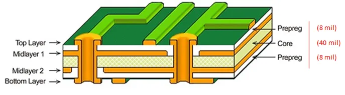
What is a 4-Layer PCB Stackup and Why is it Important for Your Design?
A 4-layer Printed Circuit Board (PCB) stackup refers to the specific arrangement of its four conductive copper layers and the insulating dielectric materials separating them. Unlike simpler two-layer boards, this configuration provides significantly more room for routing signal traces while dedicating inner layers to stable power and ground planes. This design approach is particularly beneficial for contemporary electronic applications that demand compact layouts, high-speed operation, or robust noise immunity.
The careful planning and optimization of a PCB stackup are critical for the overall performance of any electronic device. An improperly designed stackup can introduce a host of problems, including electromagnetic interference (EMI), signal crosstalk between adjacent traces, and impedance mismatches. For example, inconsistent spacing between layers can lead to signal delays or unwanted noise coupling, which directly impacts functionality. By meticulously planning the 4 layers PCB design, engineers can significantly mitigate these risks, ensuring superior signal integrity and dependable operation, especially in systems operating at frequencies exceeding 100 MHz.
Exploring Common 4-Layer PCB Stackup Configurations
When embarking on a 4-layer PCB design, the specific arrangement of layers is a pivotal decision that directly influences performance characteristics. There are two primary configurations that are widely adopted, each offering distinct advantages for different application needs. Understanding these common stackup options is the first step toward an optimized design.
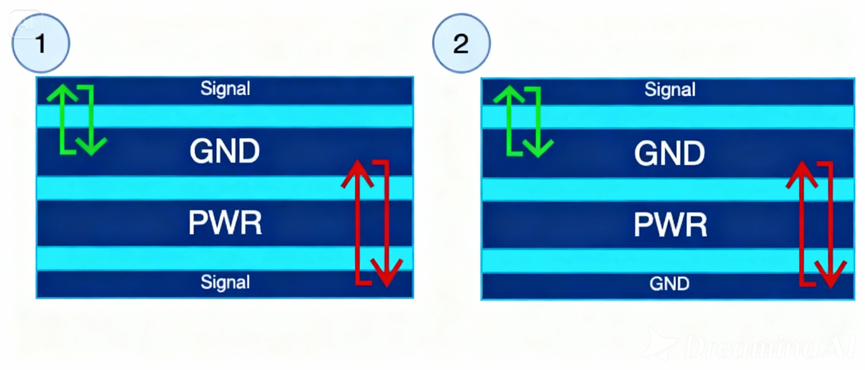
Signal-Ground-Power-Signal (SGPS) Arrangement
The SGPS configuration stands as the most frequently implemented 4-layer PCB stackup. In this setup, the outermost layers (Layer 1 and Layer 4) are designated for signal routing, providing clear paths for component connections. Critically, the second layer is a dedicated ground plane (GND), positioned directly beneath the top signal layer. The third layer functions as a power plane (VCC). This proximity of a solid ground plane to the primary signal layer offers a low-impedance return path for high-speed signals and significantly aids in electromagnetic compatibility (EMC) by reducing EMI.
This configuration is particularly well-suited for high-speed digital circuits, such as those found in microcontrollers or Field-Programmable Gate Array (FPGA) designs where operational frequencies commonly exceed 50 MHz. To maximize its benefits, AIVON’s engineering team often recommends maintaining a minimal dielectric thickness (e.g., 0.2 mm) between the top signal layer and the ground plane. This tight coupling helps in maintaining controlled impedance, typically targeting 50 ohms for critical high-speed traces, thereby preserving signal integrity.
Signal-Power-Ground-Signal (SPGS) Arrangement
An alternative, though less common, configuration is the SPGS stackup, where the power plane occupies Layer 2 and the ground plane is on Layer 3. While not as prevalent as SGPS, this arrangement can be advantageous in specific scenarios. For instance, if certain components on the top layer have substantial power requirements, placing the power plane closer can facilitate improved power delivery and distribution directly where it's needed most.
The primary benefit here lies in enhanced power delivery to components located on the top layer. This can be particularly useful in applications such as power amplifiers or other systems with significant current demands at the board's surface. However, designers must ensure that the ground plane on Layer 3 still provides an effective and continuous return path for signals routed on the bottom layer to prevent potential noise issues and maintain overall signal quality.
Key Factors for Effective 4-Layer PCB Design
Achieving an optimized PCB layer stackup goes beyond merely choosing a standard configuration; it involves a meticulous consideration of several critical design elements. Each factor plays a crucial role in ensuring the board's performance, reliability, and manufacturability.
Dielectric Material and Layer Thickness
The properties of the dielectric material, specifically its thickness and dielectric constant (Dk), profoundly influence signal impedance and propagation speed. For high-speed applications, a thinner dielectric (e.g., 0.1 to 0.2 mm) between the signal and ground layers is crucial for achieving controlled impedance, often targeted at 50 or 75 ohms for differential pairs. While standard PCB FR4 material (Dk typically 4.2-4.5) is common, higher frequency designs (above 1 GHz) benefit from low-loss materials like Rogers, which offer a lower Dk (3.0-3.5) and superior signal integrity.
Designers frequently use stackup calculator tools to precisely determine the required dielectric thickness to meet target impedance values. For instance, a 50-ohm trace on a 1.6 mm thick FR-4 board might necessitate a trace width of 0.3 mm with a 0.2 mm dielectric separation from the ground plane to achieve the desired impedance characteristics.
Integrity of Power and Ground Planes
The incorporation of dedicated power and ground planes represents a significant advantage of 4-layer PCBs. A robust, unbroken ground plane is essential for minimizing noise by providing a consistent and low-impedance return path for all signals. It is generally advisable to avoid splitting the ground plane unless absolutely necessary, as these splits can inadvertently create unintended antenna loops, thereby increasing EMI. Similarly, the power plane should be designed to be continuous and placed in close proximity to the ground plane. This arrangement effectively forms a low-inductance decoupling capacitor, which is vital for reducing power supply noise and maintaining stable voltage levels.
A practical approach to enhance power plane integrity is the strategic placement of decoupling capacitors (e.g., 0.1 μF) near the power pins of integrated circuits (ICs). These capacitors should be connected directly to both the power and ground planes using short vias to efficiently filter out high-frequency noise spikes and ensure a stable power environment for the components.
Signal Routing and Trace Layout
In a 4-layer PCB, signal traces are primarily routed on the top and bottom layers. High-speed signals, due to their sensitivity to interference, should ideally be routed on the layer closest to the ground plane—typically the top layer in an SGPS configuration—to minimize potential coupling and crosstalk. Keeping critical trace lengths as short as possible is also crucial for reducing signal propagation delays; for example, signals on FR-4 material travel approximately 150 mm per nanosecond, meaning a 150 mm trace introduces a 1 ns delay.
For differential pairs, which are common in high-speed protocols like USB or HDMI, maintaining consistent spacing (e.g., 0.2 mm) and ensuring precise length matching (within 0.5 mm) between the pair members is paramount. This careful routing prevents skew, which can degrade signal quality and lead to data errors in high-frequency data transmission.
Advanced Optimization Strategies for 4-Layer PCB Stackup
Beyond the fundamental design principles, several advanced techniques can be employed to further refine a 4-layer PCB stackup, ensuring peak performance and robust reliability. These strategies specifically address common challenges encountered in demanding electronic designs.
Minimizing Crosstalk with Optimized Layer Spacing
Crosstalk, the unwanted coupling between signals on adjacent traces or layers, can severely degrade signal integrity. In a 4-layer PCB, this is a particular concern between the top and bottom signal layers if their separation is insufficient. A key optimization involves increasing the dielectric thickness between these signal layers (e.g., to 0.8 mm or more) while simultaneously maintaining a very tight spacing between each signal layer and its adjacent ground plane (e.g., 0.2 mm). This approach effectively reduces inter-layer coupling without sacrificing the impedance control provided by the close signal-to-ground proximity.
Strategic Via Utilization
Vias, while necessary for connecting traces between different layers, introduce parasitic inductance and capacitance, which can lead to signal reflections and discontinuities. For high-speed signals, it is beneficial to use microvias or blind vias to minimize the length of the via stub, thereby reducing its inductive effects. Additionally, placing ground vias in close proximity to signal vias provides a robust return path for the signal current, preventing disruptions. Designers should also strive to limit the number of via transitions for critical signals, ideally to one or two per net, to minimize propagation delays and maintain signal integrity.
Integrated Thermal Management
In designs incorporating high-power components, effective heat dissipation is a critical concern. The dedicated power and ground planes within a 4-layer stackup can be effectively utilized as thermal spreading layers. This is achieved by connecting thermal vias from hot components directly to these planes. For example, a power IC dissipating 2 watts might require four to six thermal vias, each 0.3 mm in diameter, to efficiently transfer heat away from the component and distribute it across the larger copper planes, thus preventing localized hotspots and ensuring component longevity.
Simulation and Rigorous Testing
Prior to finalizing any 4-layer PCB stackup, it is highly recommended to leverage simulation tools. These tools can model signal integrity and impedance characteristics, predicting potential issues such as ringing or overshoot in high-speed signals. This predictive capability allows designers to make necessary adjustments to layer spacing or trace widths before fabrication. Following PCB manufacturing, thorough testing with an oscilloscope is essential to verify signal quality. Designers should look for clean signal edges with rise times under 1 nanosecond for high-speed signals, confirming that the physical board performs as intended by the simulations.
Common Pitfalls to Avoid in 4-Layer PCB Stackup Design
Even experienced designers can encounter challenges when planning a PCB layer stackup. Being aware of frequent mistakes can help prevent costly redesigns and performance issues.
Neglecting Ground Plane Continuity
One of the most critical errors is unnecessarily splitting the ground plane to facilitate routing. While seemingly convenient, breaking the ground plane disrupts the continuous return path for signals, leading to increased noise, electromagnetic interference (EMI), and potential ground bounce. A continuous, solid ground plane should always be prioritized.
Inadequate Impedance Control
Failing to properly calculate trace width and layer spacing for controlled impedance is a common oversight, particularly in high-speed designs. When impedance is not matched to the transmission line, signal quality degrades, leading to reflections, ringing, and data errors, especially at frequencies above 100 MHz.
Overloading Signal Layers
Attempting to route too many signal traces on a single layer can lead to high trace density, making it difficult to maintain adequate spacing and increasing the likelihood of crosstalk. Signals should be distributed evenly between the top and bottom layers to prevent congestion and optimize performance.
Poor Via Placement
Placing vias far from their associated ground or power planes can create undesirable inductive stubs and disrupt the integrity of signal return paths. This poor placement can introduce noise and signal integrity issues. Vias should always be placed in close proximity to their reference planes to ensure a solid return path.
Applications Benefiting from 4-Layer PCB Stackups
A meticulously designed 4-layer PCB stackup offers exceptional versatility and is ideally suited for a broad spectrum of electronic applications that demand high performance, compact size, and reliability.
Consumer Electronics
Modern consumer devices, such as smartphones, tablets, and wearable technology, heavily rely on 4-layer PCBs. These designs enable the integration of numerous high-speed digital signals and complex power distribution networks within extremely compact form factors, facilitating the advanced functionalities users expect.
Industrial Control Systems
In industrial settings, applications like Programmable Logic Controllers (PLCs) and automation systems benefit significantly from the enhanced noise immunity provided by the dedicated ground and power planes in a 4-layer stackup. This robustness is critical for reliable operation in electrically noisy environments where precision and uninterrupted functionality are paramount.
Automotive Systems
Automotive electronics, including Engine Control Units (ECUs) and various sensor modules, frequently incorporate 4-layer PCB designs. The increased routing capabilities and improved signal integrity contribute to the reliability and performance required for safety-critical systems operating in harsh and demanding vehicle environments.
Conclusion: Elevating Your 4-Layer PCB Design
Optimizing a 4-layer PCB stackup is a complex yet rewarding endeavor, involving a careful balance between ensuring signal integrity, mitigating noise, and maintaining manufacturability. By selecting an appropriate configuration, such as the widely adopted Signal-Ground-Power-Signal stackup, and meticulously addressing critical factors like layer spacing, via placement, and impedance control, designers can craft boards that perform reliably even in the most demanding applications.
Remember to incorporate robust simulation tools into your workflow, thoroughly test proto board, and actively avoid common pitfalls like splitting ground planes or overlooking thermal management needs. Whether your project involves high-speed digital circuits or power-intensive systems, a well-conceived PCB layer stackup forms the bedrock of success. Employ the insights and strategies detailed in this guide to refine your 4-layer PCB design process and achieve superior outcomes for your next electronic venture.