Introduction
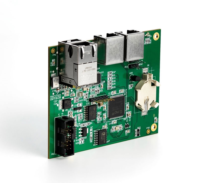
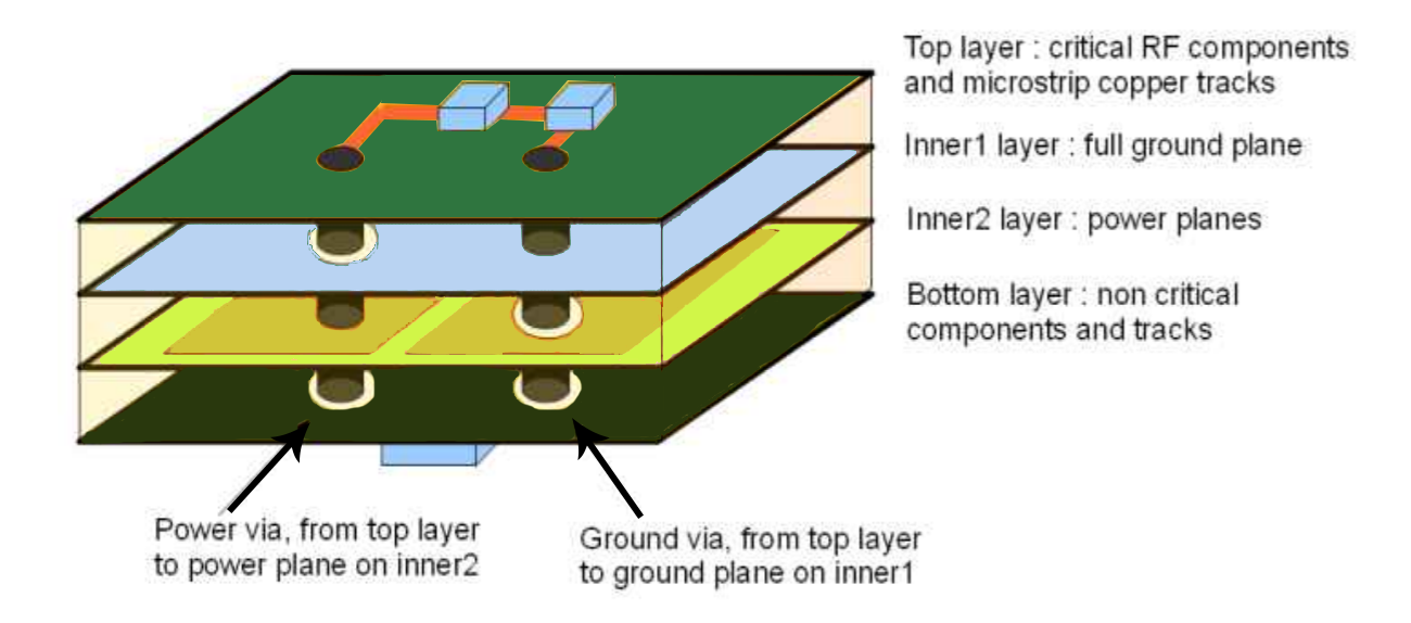
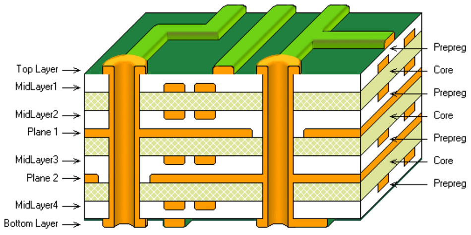
Four-layer PCBs represent the most common stack-up beyond two layers in modern digital and mixed-signal designs. The typical configuration uses top signal, ground plane, power plane, and bottom signal. This structure provides excellent noise immunity and controlled impedance, yet designers frequently encounter 4-layer PCB routing challenges when component density increases. Congested BGA breakouts, multiple voltage domains, high-speed interfaces, and the need to minimize layer hopping all demand disciplined planning. This article examines the core difficulties in 4-layer PCB trace routing and presents proven, standard-compliant solutions.
Common 4-Layer PCB Routing Challenges
Limited Routing Channels
Only two signal layers exist for all traces. Dense BGA fanouts quickly consume available space, especially under 0.8 mm pitch devices.
Signal Crossing and Layer Hopping
Two signals that must cross on the same layer require vias to the opposite signal layer. Excessive layer hopping creates via stubs, increases inductance, and complicates return current paths.
Power Distribution Constraints
The dedicated power plane often carries multiple voltage rails. Splitting the plane creates narrow necks and slots that fragment return paths for high-speed signals.
Ground Plane Integrity
Large cuts in the ground plane for through-hole components or vertical routing destroy low-inductance return paths and increase EMI.
Crowded Designs with Mixed Technologies
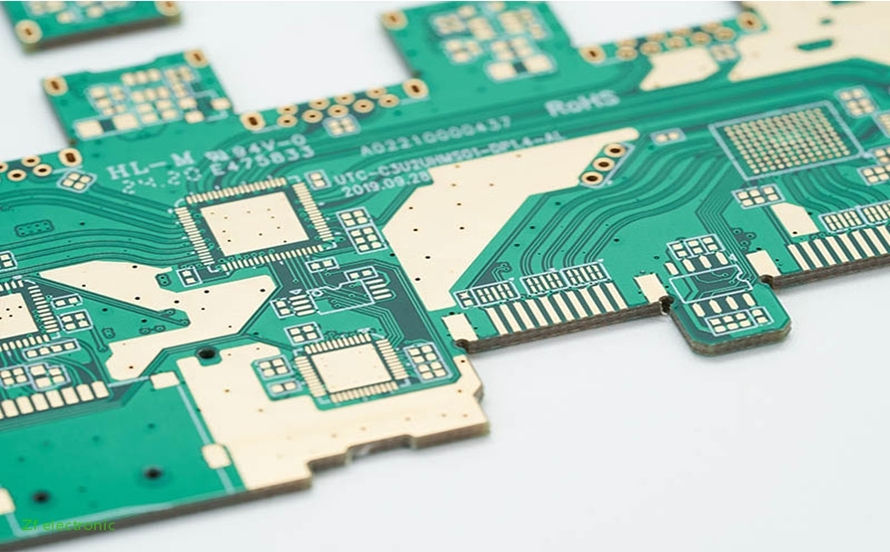
Combining fine-pitch digital ICs, analog sections, and large connectors on four layers forces difficult trade-offs between routing density and signal integrity.
Effective 4-Layer Routing Strategies
Pre-Planning and Component Placement
- Group related circuits to minimize inter-area routing
- Align high-speed interfaces along board edges for shortest paths
- Place decoupling capacitors directly adjacent to IC power pins
- Orient BGAs to allow natural X/Y breakout directions
Intelligent Layer Assignment
Reserve the bottom layer primarily for horizontal traces and the top layer for vertical traces (or vice versa). This H-V routing discipline reduces the need for layer changes by 60–80% in most designs.
Via Management Techniques
- Use blind or buried vias only when absolutely necessary due to PCB cost
- Place vias in a regular grid pattern for easier routing continuation
- Share vias between multiple signals when traces run parallel (via stitching)
- Minimize stub length by routing critical signals on the layer farthest from via termination
Power Plane Partitioning Rules
- Keep power islands as large and rectangular as possible
- Maintain at least 20 mm separation between different voltage domains
- Route high-current traces on signal layers instead of narrow plane necks
- Add stitching capacitors across plane splits for high-frequency return paths
Ground Plane Protection
- Route all signals over intact ground plane whenever possible
- Use ground fill on signal layers connected by via stitching every 10–15 mm
- Avoid routing traces under sensitive analog or RF components
High-Speed Signal Considerations on 4 Layers
Critical interfaces such as USB, HDMI, DDR, and Ethernet require controlled impedance and continuous return paths.
Practical Solutions
- Route differential pairs on the same layer adjacent to the reference plane
- Avoid crossing plane splits with high-speed signals
- Use 45-degree angles instead of 90-degree corners
- Maintain constant trace width and spacing throughout the route
- Add guard traces or stitching vias along long parallel runs when needed
Thermal and Mechanical Balance
Symmetric copper distribution across layers prevents board warpage during reflow. Balance large copper pours on top and bottom layers. Mirror power and ground plane coverage as closely as possible.
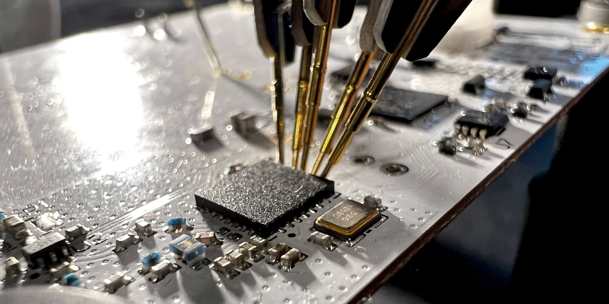
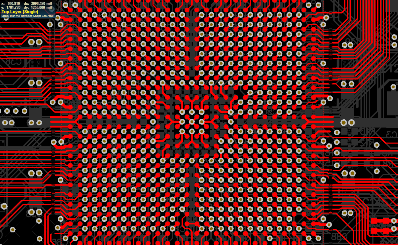
Real-World Example: Routing a 0.8 mm Pitch BGA on 4 Layers
A typical 256-ball BGA requires approximately 160 signals. Using dog-bone fanout with via-in-pad on outer rows allows all signals to escape on 4 layers PCB without neck-down below 0.1 mm trace width. Inner signals route diagonally between vias on the opposite layer. Careful pre-planning of pin assignment reduces total via count by 25–30%.
Conclusion
Successful 4-layer PCB routing demands strict discipline from the earliest placement stage. Horizontal-vertical routing discipline, intelligent via placement, and protection of reference plane integrity solve the majority of 4-layer PCB trace routing challenges. When density exceeds practical limits on four layers, designers must accept either relaxed timing margins or migration to six layers. With proper constraints and guidelines, four layers remain perfectly adequate for most consumer, industrial, and communication products operating below 2–3 GHz.
FAQs
Q1: How many signals can realistically escape a 0.8 mm BGA on 4 layers?
A1: Approximately 180–220 signals escape comfortably using dog-bone fanout and via-in-pad on outer rows while maintaining 0.1–0.12 mm trace/space rules.
Q2: Is it acceptable to cross power plane splits with high-speed signals on 4-layer boards?
A2: No. Crossing a split forces return current to detour around the gap, creating large loop area and EMI. Route around the split or add stitching capacitors.
Q3: When should I consider moving from 4 layers to 6 layers?
A3: Move to six layers when BGA pitch drops below 0.65 mm, when multiple high-speed interfaces exist, or when power distribution requires more than three distinct voltages with clean separation.
Q4: Does horizontal-vertical routing really reduce via count that much?
A4: Yes. Following strict H-V discipline typically reduces total vias by 50–80% compared to free-angle routing on both layers.
References
IPC-2221B — Generic Standard on Printed Board Design. IPC, 2015.
IPC-2141A — Design Guide for High-Speed Controlled Impedance Circuit Boards and Hybrids. IPC, 2004.
IPC-6012E — Qualification and Performance Specification for Rigid Printed Boards. IPC, 2017.
IPC-TM-650 2.6.27 — Characteristic Impedance and Time Delay of Transmission Lines. IPC, 2019.