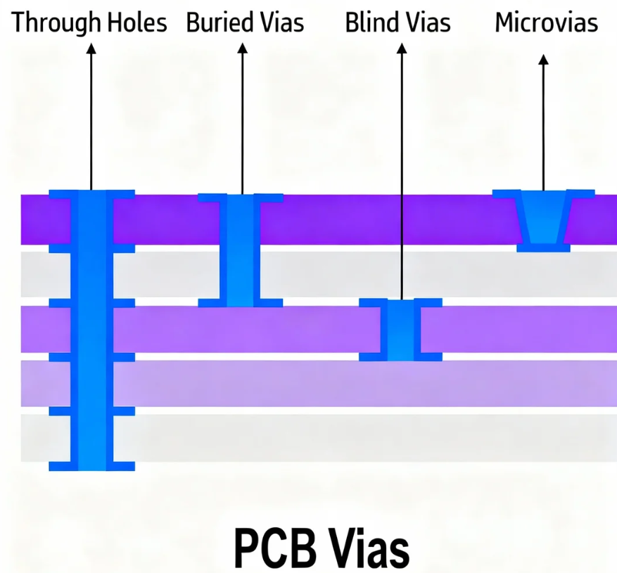
What Are Stacked Vias in High-Density PCBs?
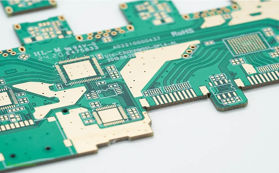
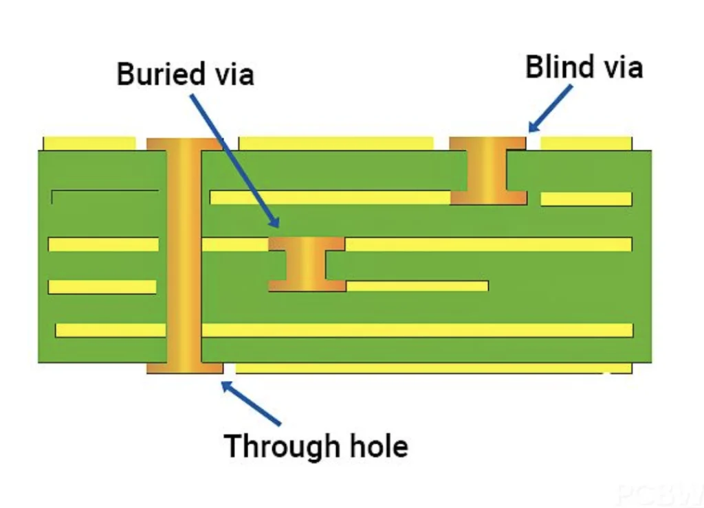
Stacked vias represent a sophisticated interconnection method within High-Density Interconnect (HDI) Printed Circuit Boards (PCBs). Unlike conventional through-hole vias that penetrate all layers, stacked vias are composed of multiple microvias, precisely positioned directly atop one another. These microvias create a vertical conductive path that connects specific internal layers without occupying excessive horizontal board space.
This technique is fundamental to achieving higher component densities and more compact electronic devices. In an HDI PCB stacked via configuration, each microvia segment is typically filled with a conductive material, often copper, ensuring robust electrical continuity through the stack. Such designs are essential for modern electronics, including smartphones, advanced medical devices, and other compact, high-performance gadgets where board real estate is at a premium.
Why Integrate Stacked Vias into PCB Designs?
Stacked vias offer significant engineering advantages, making them a preferred choice for advanced PCB layouts. Their implementation directly contributes to enhancing board functionality within constrained physical dimensions. The ability to route connections vertically through multiple layers without large via footprints allows for more intricate circuit designs and shorter signal paths.
The primary motivations for using stacked vias include substantial space savings, which enables the creation of smaller and lighter products, and marked improvements in signal integrity. By minimizing the length of conductive traces, these vias help reduce issues like impedance mismatch and signal attenuation, especially crucial for high-speed digital and RF applications operating above 1 GHz. This capability supports a greater density of active components and more complex circuitry on a single board.
How Do Stacked Vias Reduce Board Footprint?
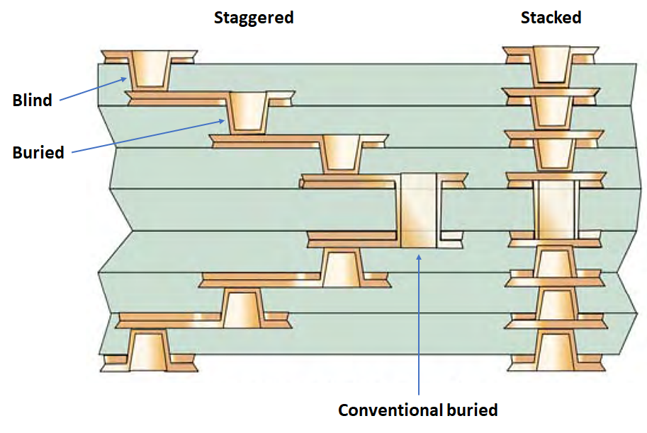
By stacking multiple microvias, designers can establish connections between numerous layers directly beneath a component, freeing up valuable routing channels on external layers. This vertical integration drastically decreases the overall PCB footprint compared to using staggered or through-hole vias that require more lateral space. This space efficiency is paramount for devices like wearables and portable medical equipment, where every millimeter counts.
How Do Stacked Vias Improve Signal Quality?
The compact, vertical structure of stacked vias leads to shorter electrical paths compared to alternative via types. Shorter paths inherently reduce parasitic capacitance and inductance, which can degrade signal quality in high-frequency applications. This reduction in parasitic effects helps maintain signal integrity, minimizing crosstalk and reflections, thus ensuring more reliable and faster data transmission within the PCB.
Key Considerations for Designing with Stacked Vias
Implementing stacked vias effectively demands meticulous planning and adherence to specific design principles. These guidelines ensure both the performance and manufacturability of HDI PCB stacked via structures. Close attention to detail in the design phase can prevent high pcb cost and ensure optimal board functionality.
Understanding Your Layer Stack-Up and Via Placement
Before integrating stacked vias, a thorough understanding of the PCB's layer stack-up is essential. Designers must precisely determine which layers need to be interconnected and strategically place vias to optimize routing. For instance, a common HDI stack-up might be described as 2+N+2, indicating two outer layers built up with microvias around a core (N) of internal layers. Stacked vias should only be utilized where their benefits—such as space savings or improved signal integrity—are clearly justified to avoid unnecessary manufacturing complexity.
Optimizing Via Dimensions and Aspect Ratio
The physical dimensions of microvias are critical. Diameters typically range from 0.1 mm to 0.15 mm. A crucial parameter is the aspect ratio, defined as the via's depth-to-diameter. This ratio should ideally be 1:1 or less to facilitate complete and reliable copper plating during manufacturing. For example, a 0.1mm diameter microvia should not exceed 0.1mm in depth to ensure proper filling and avoid voids, which could compromise the electrical connection and structural integrity.
Ensuring Precise Alignment
Accurate alignment of stacked vias is non-negotiable. Even slight misalignments between successive microvias can lead to connection failures. Modern CAD tools provide advanced features for precise via alignment and error checking, which are indispensable for HDI designs. Designers should leverage these tools to maintain tight tolerances and ensure each via segment in the stack is perfectly centered above the one below it.
Managing Signal Integrity for High-Speed Applications
For designs involving high-speed signals, stacked vias can introduce subtle parasitic effects. To mitigate these, it's advisable to limit the height of via stacks—typically to no more than 2-3 vias. Additionally, strategically placing ground planes adjacent to high-speed signal layers can significantly reduce interference and help maintain signal integrity by providing a clear return path.
The Manufacturing Process for Stacked Vias
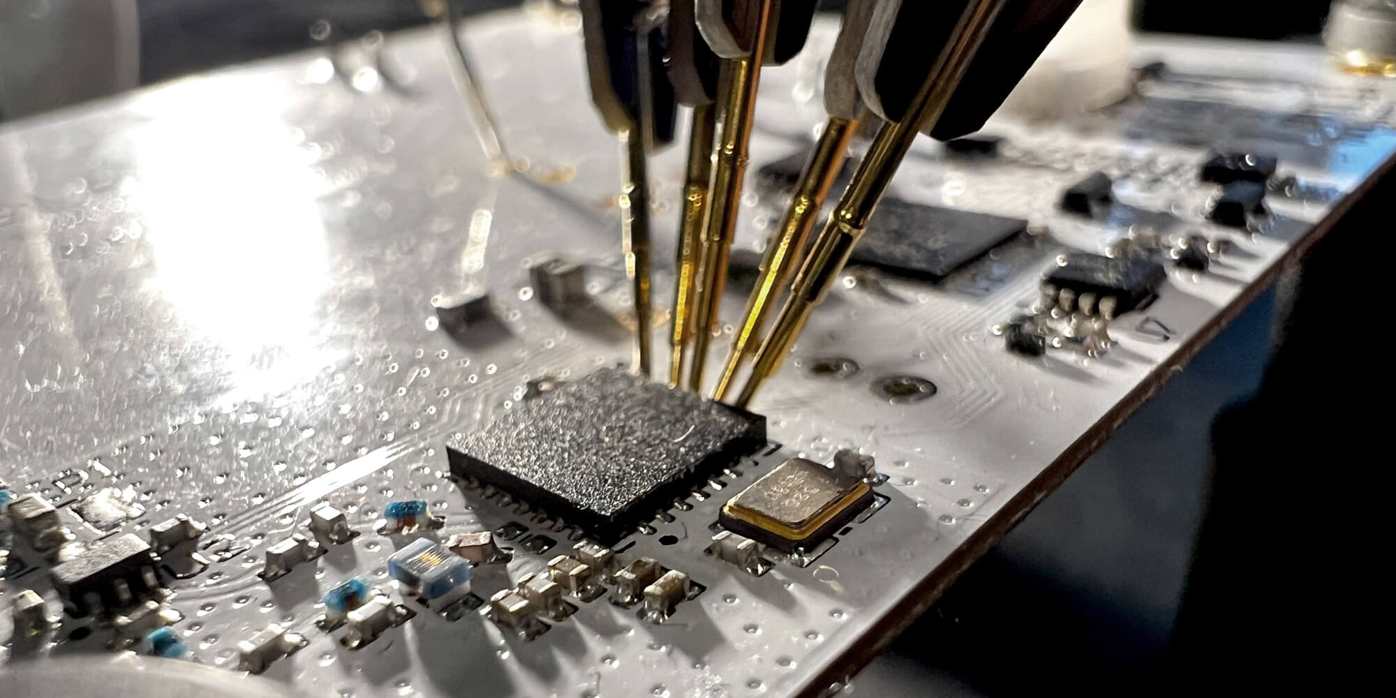
The production of stacked vias in HDI PCBs is a multi-stage, precise operation that differs significantly from conventional PCB fabrication. It relies on advanced techniques to create the intricate vertical interconnections.
Sequential Build-Up and Laser Drilling
HDI PCBs are constructed using a sequential lamination process, where layers of dielectric material and copper are added incrementally. Each layer is meticulously aligned before microvias are formed. Microvias are typically created using highly focused laser drilling, which offers superior precision compared to mechanical drilling. Laser drilling produces clean, small-diameter holes (as fine as 0.1 mm) without damaging the surrounding laminate material, which is crucial for the integrity of the stacked structure.
Copper Plating and Filling
Following laser drilling, the microvias undergo a copper plating process to establish electrical conductivity. In stacked via designs, it is common practice to fill these microvias entirely with copper. This filling process ensures a solid, void-free connection that enhances both electrical reliability and mechanical robustness, preventing potential structural weaknesses. This step is critical for the long-term performance of the board.
Repeated Lamination and Stacking
Once the microvias for a specific layer pair are drilled, plated, and filled, subsequent layers are laminated on top. This sequential process is repeated for each segment of the stacked via. Extreme precision is maintained throughout these lamination cycles to prevent any misalignment between the stacked microvias, which could result in open circuits or compromised electrical connections.
Addressing Reliability Concerns in Stacked Via Designs
While stacked vias offer numerous advantages, their unique construction introduces specific reliability challenges. Proactive design and manufacturing strategies are necessary to ensure their long-term performance.
Mitigating Thermal Stress
PCBs are subject to thermal cycling during operation, leading to expansion and contraction of materials. Stacked vias, particularly due to their small size and multi-layer structure, can be susceptible to cracking under these thermal stresses. To counteract this, designers should select dielectric and copper materials with closely matched Coefficients of Thermal Expansion (CTE). For example, choosing a dielectric with a CTE near that of copper (approximately 17 ppm/°C) can significantly reduce internal stresses within the via structure.
Preventing Copper Filling Defects and Misalignment
Incomplete copper filling or the presence of voids within stacked vias can create weak points that lead to premature failure. Manufacturers employ advanced plating techniques and utilize X-ray inspection methods to detect and prevent such defects. Designers can contribute by adhering to recommended via aspect ratios, which facilitate proper copper deposition. Furthermore, maintaining tight manufacturing tolerances for via placement, such as ±0.05 mm, and providing clear design files, helps prevent misalignment, a common cause of poor electrical connections. Collaborative efforts with manufacturing partners are essential to address these issues effectively.
Economic Factors of Stacked Via Implementation
The decision to use stacked vias often involves a trade-off between advanced performance capabilities and increased manufacturing costs. Understanding the elements that influence these costs is vital for project budgeting and determining the overall value proposition.
What Drives Up the Cost of Stacked Vias?
Several factors contribute to the higher cost of stacked via PCBs. The sequential build-up process, which involves multiple lamination and drilling cycles, directly correlates with the number of layers and overall manufacturing complexity. Laser drilling, required for microvias, is inherently more expensive than traditional mechanical drilling due to the precision and specialized equipment involved. Furthermore, the necessity for precise copper filling and advanced material selections, such as low-loss dielectrics or those with tailored CTEs, adds to material expenses. Finally, manufacturing yields for complex HDI designs can be lower, spreading setup costs over fewer usable boards, thus increasing the per-unit cost. For instance, a 10-layer HDI board with stacked vias might incur 30-50% higher costs than a simpler 6-layer board.
Balancing Performance Needs with Budget Constraints
While the investment in stacked vias is significant, their benefits in terms of miniaturization and enhanced performance are often critical for high-end applications like aerospace, medical implants, or advanced consumer electronics. In these sectors, the performance gains typically justify the added expense. For projects with stricter cost constraints, designers might explore alternatives such as staggered vias, where microvias are offset rather than stacked, which can reduce manufacturing complexity and associated costs while still achieving a high-density layout.
Applications and Manufacturer Collaboration for Stacked Vias
Stacked vias are integral to various cutting-edge electronic products, enabling performance and form factors previously unattainable. Effective communication with manufacturing partners is crucial for successful implementation.
Where Are Stacked Vias Most Commonly Used?
Stacked vias are prevalent in industries demanding compact, high-performance electronics. This includes consumer devices like smartphones, tablets, and wearable technology, where space is severely limited. In the automotive sector, they are crucial for advanced driver-assistance systems (ADAS) and infotainment units, ensuring reliable, high-speed data transfer. Medical devices, such as portable diagnostic tools and implantable electronics, benefit from the miniaturization and reliability offered by stacked via designs. Furthermore, the aerospace and defense sectors utilize these high-density interconnects in satellites and mission-critical military equipment to meet stringent performance and reliability standards.
Effective Collaboration with PCB Manufacturers
To ensure the successful integration of stacked vias, close collaboration with your PCB manufacturer is indispensable. Designers should provide comprehensive and accurate design files that detail via specifications, the complete layer stack-up, and precise material requirements. It's advisable to discuss the manufacturer's capabilities early in the design cycle, verifying their minimum via size and stacking limits. Requesting Design for Manufacturability (DFM) feedback is also highly recommended, as manufacturers can identify potential issues related to via alignment, aspect ratios, or material compatibility before production commences. Finally, establishing clear testing protocols, including X-ray inspections for void detection, in conjunction with your manufacturer, helps guarantee the reliability of the stacked vias.
Conclusion: Mastering Stacked Vias for Advanced PCB Design
Stacked vias are a transformative technology for high-density PCBs, enabling the development of smaller, faster, and more powerful electronic devices. By diligently applying best practices in design, understanding the intricate manufacturing processes, and proactively addressing reliability concerns, engineers can effectively leverage stacked vias to optimize their HDI PCB layouts. While the cost implications require careful consideration, the performance advantages often make them an invaluable choice for cutting-edge applications. Mastering the complexities of stacked via technology is key to pushing the boundaries of electronic design and bringing innovative product concepts to fruition.