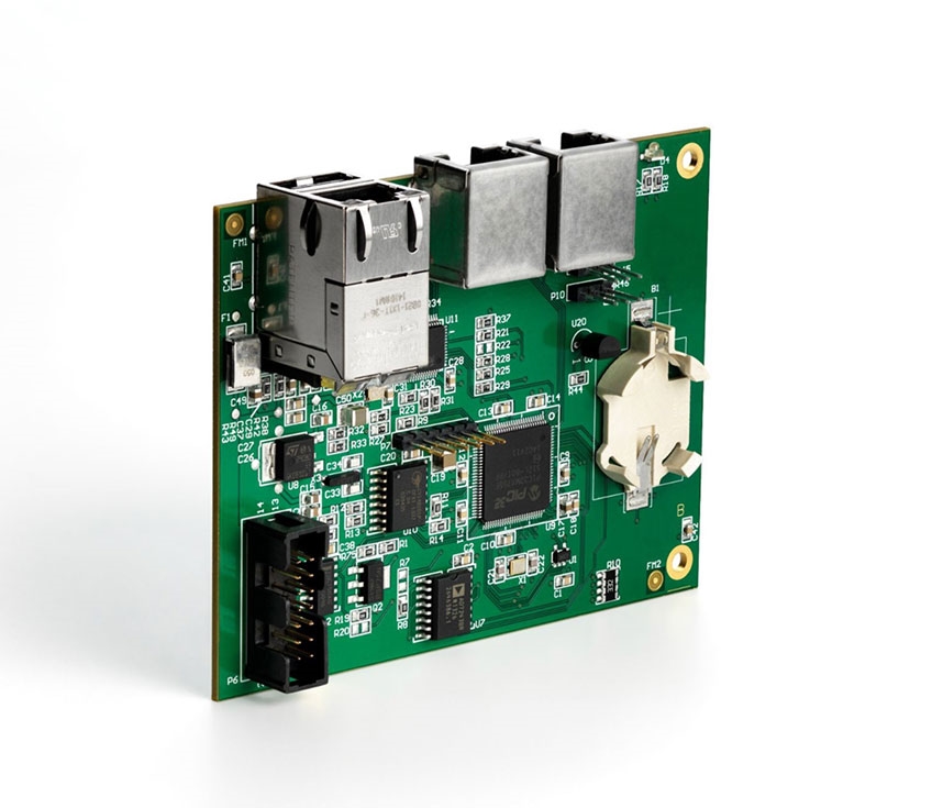
Introduction
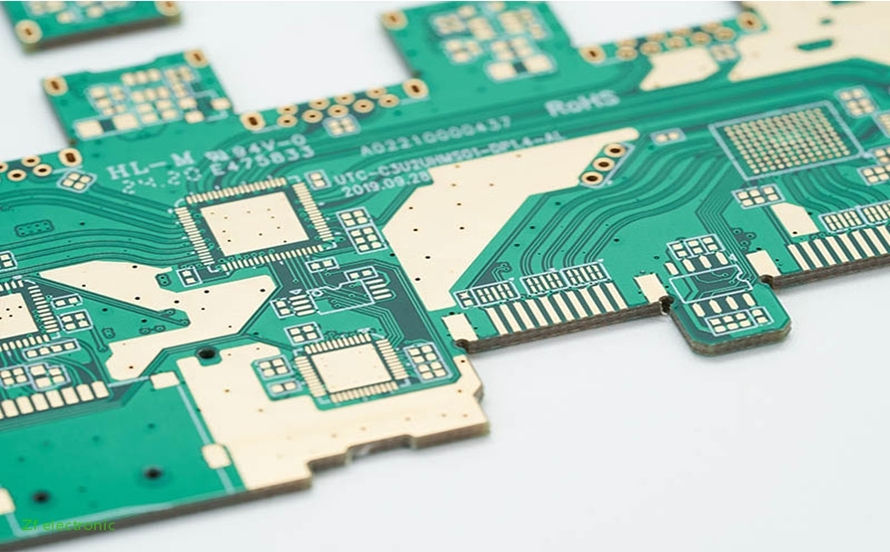
Multi-layer PCBs with six or more layers contain buried and blind vias, microvias, and high-density interconnect structures that are invisible from the surface. Traditional visual inspection cannot verify inner-layer registration, plating quality, or via integrity. Modern multi-layer PCB testing and inspection combine optical, X-ray, electrical, and functional methods to guarantee performance before assembly. IPC-6012E and IPC-A-600K define the acceptance criteria for each technique. This article presents the standard-compliant inspection sequence used in volume production to achieve zero electrical defects.
Standard Inspection and Testing Flow
- Incoming material verification
- Post-lamination dimensional and registration check
- Drilling quality and hole-wall integrity
- Plating thickness and void inspection
- Final electrical testing
- Automated Optical Inspection (AOI)
- X-ray inspection (sampling or 100 %)
- Microsection analysis (first article and periodic)
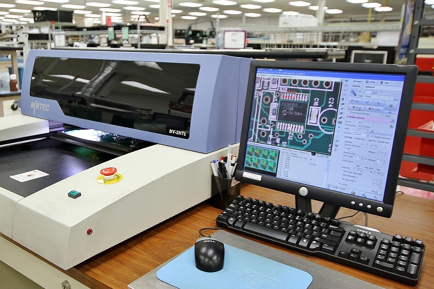
Automated Optical Inspection (AOI) for Multi-Layer PCBs
AOI systems compare the finished board against the Gerber data at 5–15 µm resolution.
Primary detection capability on outer layers:
- Line width and spacing violations
- Missing or excess solder mask
- Solder mask registration errors
- Surface contamination and scratches
Limitations: AOI cannot see buried features or inner-layer defects. It serves as the first line of outer-layer quality control before electrical test.
X-Ray Inspection Methods
2D Real-Time X-Ray
Used for 100 % inspection of BGA voiding and via fill in volume production.
3D Computed Tomography (CT)
Provides full volumetric reconstruction. Essential for stacked microvia reliability validation.
Typical X-Ray Inspection Targets
- Plated-through hole wall thickness and voids
- Buried and blind via fill percentage (IPC-6012E requires ≥ 75 % copper fill for Type VI and VII vias)
- Inner-layer registration and annular ring centering
- Barrel cracking after thermal stress
- Solder joint voiding under large thermal pads
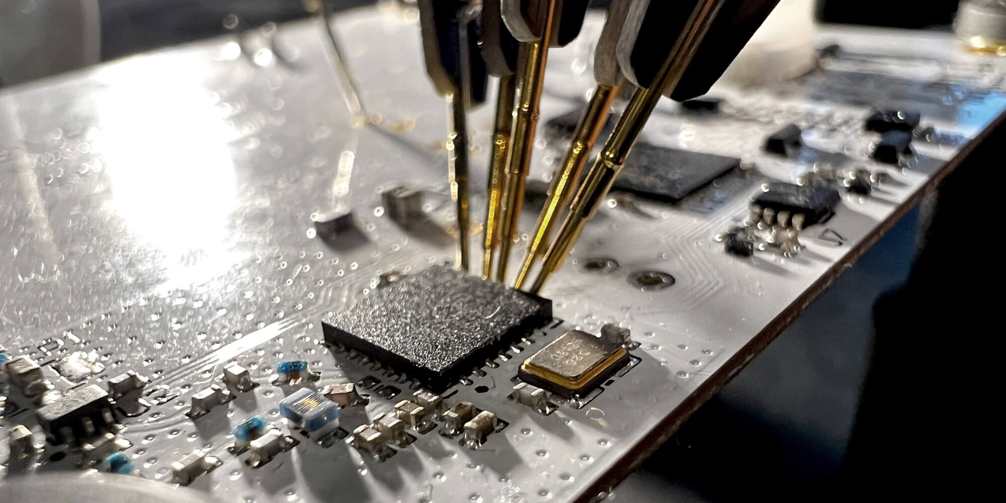
Electrical Testing Techniques
Flying Probe Testing
- Ideal for prototypes and low-to-medium volume
- No fixture cost
- Tests continuity, isolation, and embedded passives
- Typical net count limit ≈ 20,000
Dedicated Bed-of-Nails Fixture Testing
- Fastest for high-volume production
- 100 % continuity and isolation
- Can include high-voltage HiPot and 4-wire Kelvin measurement
- Fixture build requires 4–6 weeks lead time
IPC-9252A defines electrical test requirements and acceptable resistance limits.
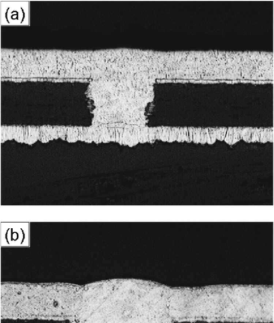
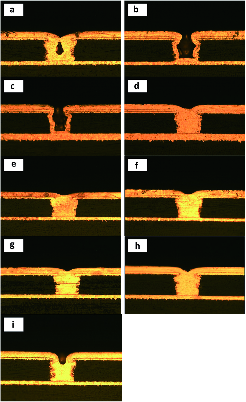
Microsection Analysis (Cross-Sectioning)
Performed on first article and periodic coupons per IPC-TM-650 2.1.1.
Key measurements:
- Copper plating thickness (minimum 20 µm average, 15 µm minimum in holes)
- Dielectric spacing between layers
- Via fill percentage and void content
- Inner-layer copper foil thickness and etch-back
- Solder mask thickness and coverage over knees
Additional Advanced Methods
Impedance Testing (TDR)
Verifies controlled-impedance traces meet ±10 % tolerance using Time Domain Reflectometry per IPC-TM-650 2.5.5.7.
Thermal Stress Testing
Float at 288 °C for 10 seconds × 6 cycles per IPC-TM-650 2.6.8 to reveal plating cracks and separation.
Automated Acoustic Microscopy (C-SAM)
Non-destructive detection of delamination and large voids in thick boards.
Acceptance Criteria Summary (IPC-6012E)
| Feature | Class 2 Requirement | Class 3 Requirement |
|---|---|---|
| Minimum annular ring | 50 µm (external) | 50 µm (external) |
| Plated hole copper | 20 µm average | 25 µm average |
| Buried via fill | Not specified | |
| Dielectric spacing | ≥ 90 µm | ≥ 100 µm |
| Registration (layer-to-layer) | ≤ 100 µm | ≤ 75 µm |
Conclusion
Multi-layer PCB performance and reliability depend on systematic inspection at every critical process step. AOI verifies outer-layer quality, X-ray confirms hidden via and plating integrity, electrical testing guarantees net continuity, and microsection validates process capability. Implementing all four methods in sequence consistently achieves defect rates below 50 ppm in high-volume production while meeting the most demanding automotive and aerospace requirements.
FAQs
Q1: Is X-ray inspection mandatory for all multi-layer PCBs?
A1: Not for simple 4–6 layer boards with only through vias. X-ray becomes mandatory when using blind/buried vias, stacked microvias, or via-in-pad structures.
Q2: Can flying probe replace a bed-of-nails fixture completely?
A2: Flying probe is excellent for prototypes and NPI but becomes too slow above 500–1000 boards per batch. Fixture testing remains the standard for volume production.
Q3: How often should microsection analysis be performed?
A3: First article on every new build plus one coupon per panel on every production lot, or minimum once per shift for continuous runs.
Q4: Does AOI replace final visual inspection on multi-layer boards?
A4: AOI replaces 90–95 % of manual visual inspection on outer layers but cannot detect inner-layer defects or plating quality. Final visual remains required per IPC-A-600K.
References
IPC-6012E — Qualification and Performance Specification for Rigid Printed Boards. IPC, 2017.
IPC-A-600K — Acceptability of Printed Boards. IPC, 2020.
IPC-TM-650 2.1.1 — Microsectioning. IPC, 2014.
IPC-TM-650 2.6.27 — X-Ray Inspection. IPC, 2019.
IPC-9252A — Requirements for Electrical Testing of Unpopulated Printed Boards. IPC, 2016.