Introduction
As control requirements for devices increase, more power switch circuits appear in product designs. Their objectives vary: some require fast on/off transitions, some require low on-resistance plus high current, and some require zero idle power. Although application needs differ, MOSFETs are commonly used for switching.
The following describes several MOSFET-based power switch topologies commonly used in product designs.
1. NMOS Low-Side Power Switch
(Low-side drive; simplest and most practical, but not suitable for every circuit and may affect the operation of some systems.)
NMOS and PMOS differ in device physics and process. For a given cost, NMOS devices typically offer faster switching, higher rated current, and lower on-resistance, so NMOS is usually preferred in designs.
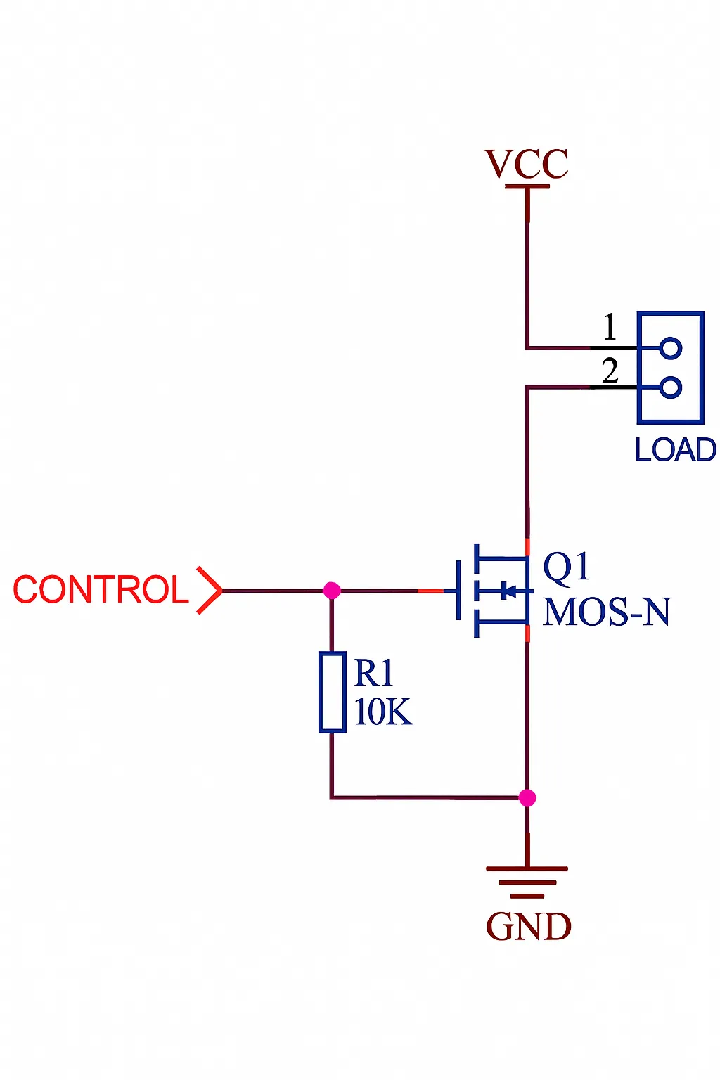
Typical low-side NMOS switch: the control signal labeled CONTROL is usually 3–12 V. One side of the load connects to the positive supply and the other to the NMOS drain. When CONTROL is high, Vgs > NMOS threshold and the MOSFET conducts, so the load operates. When CONTROL is low, Vgs = 0 and the MOSFET is off, so the load stops.
1.1 Design considerations
1.1.1 Gate discharge resistor R1
It is common to place a resistor of about 10 kΩ between the NMOS gate and source to bleed gate charge. The gate-to-source impedance is very high (typically megaohms or more) and there is gate capacitance, so without a bleed resistor the gate charge can remain for a long time. If the control signal is removed after being driven high, the gate capacitance can keep Vgs above threshold and the load may continue to run. The bleed resistor speeds discharge and makes the circuit behavior more predictable.
1.1.2 Vgs range: effect on conduction speed and on-resistance
Larger packages such as TO-220, TO-251AA, SOP-8, SO-8, DFN, TO-252, TO-263 typically have a maximum Vgs rating around ±20 V. SOT-23 devices often have a maximum Vgs around ±12 V. Higher Vgs reduces Rds(on) and increases switching speed, which is why motor control applications often use 12 V gate drive. Do not exceed the manufacturer-specified Vgs limits or the MOSFET may be damaged.
1.1.3 Parasitic capacitances, drive current, and gate drivers
1.1.3.1 Parasitic capacitance and switching speed
The gate-to-source parasitic capacitance affects turn-off and turn-on speed. Smaller capacitance yields faster switching and lower switching loss. Choose devices with lower gate charge when fast switching is required.
1.1.3.2 Gate charge, switching frequency, and drive current needs
The MOSFET gate appears mainly as a capacitance. At low frequency the required drive current is small, but as switching frequency rises, the capacitive charging/discharging frequency increases and the capacitive reactance decreases. At higher PWM frequencies the required gate drive current can become much larger. A microcontroller GPIO that can supply a few milliamps is often insufficient; direct driving from the MCU can overload the MCU pin and distort the waveform, which may prevent reliable MOSFET switching.
This occurs commonly in motor control or power conversion, where control signals are PWM in the tens of kHz to MHz range. In those cases use a dedicated MOSFET gate driver IC. Low-side gate drivers are simple (often a half-bridge internally). Many products use combined high-side and low-side gate driver ICs. For single low-side driving, an NP transistor pair can sometimes approximate the required performance, but dedicated drivers are preferred for high-frequency, high-current applications.
2. NMOS High-Side Power Switch
(High-side drive; stable and higher performance)
Low-side NMOS switching floats the ground of the load. That may be acceptable in many circuits, but not in designs that require low-side current sensing or a fully disconnected supply. For those cases a high-side switch is required.
Driving an NMOS as a high-side switch usually requires an additional gate driver IC. There are two common approaches:
- Integrated charge pump high-side driver: includes an internal charge pump to provide a gate drive above Vbus, allowing continuous on-time (100% duty). This approach is stable but the gate driver cost is higher.
- Bootstrap capacitor (bootstrap) gate driver: uses a floating bootstrap capacitor that is charged while the low-side device is active. This approach requires PWM so the bootstrap capacitor can recharge during the off portion of the cycle, and typically cannot support 100% duty cycle without special handling.
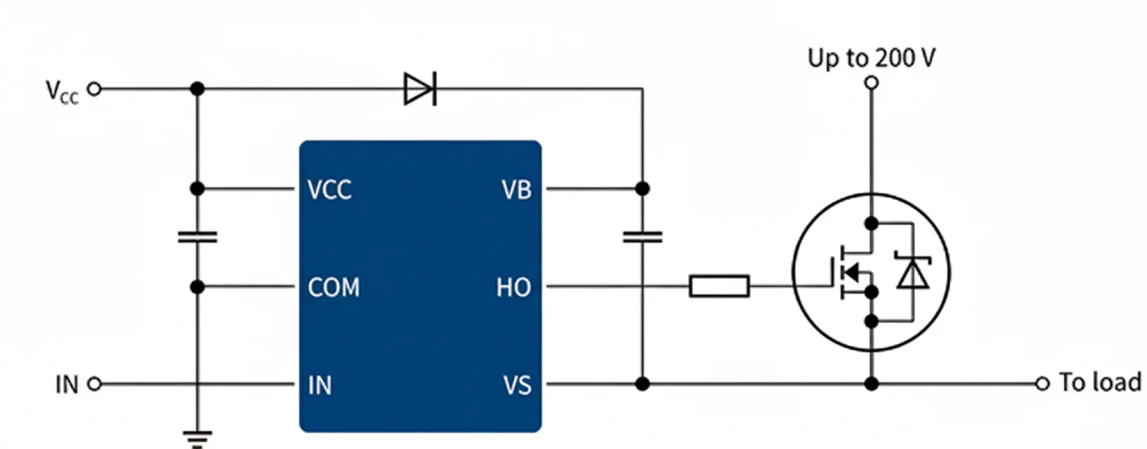
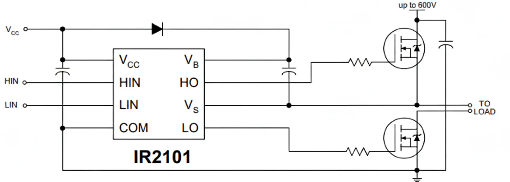
Bootstrap capacitor circuit principle
Bootstrap drives are common in motor control and power conversion. Many driver ICs integrate both high-side and low-side drivers with dead-time control to prevent simultaneous conduction of both transistors in a half-bridge. Common driver IC references include IR2101, IR2104, IR2110, IR2130; many commercial gate drivers are based on these architectures.
The bootstrap mechanism provides isolated gate drive voltage and manages charging/discharging of the bootstrap capacitor. Using the IR2101 as an example:
- When HIN is low, the high-side MOSFET is off and the low-side MOSFET is on. The external high-side MOSFET gate is pulled down via the internal low-side path so the external high-side MOSFET is off. At this time the half-bridge output is approximately 0 V, so the bootstrap capacitor can be charged through the diode into the bootstrap capacitor.
- When HIN is high, the high-side MOSFET turns on and the low-side MOSFET turns off. The bootstrap capacitor then provides gate drive to the external high-side MOSFET via the Vb -> HO path, allowing the high-side MOSFET to remain on until the bootstrap voltage decays. Because the gate-source leakage is small, the external high-side MOSFET can remain on for a long time within the limits of the bootstrap reservoir.
Since HIN/LIN are PWM and the bootstrap capacitor is recharged during off periods, the input duty cycle is generally limited below 100% (practical limit often 99% or less) to ensure the bootstrap capacitor is replenished each cycle.
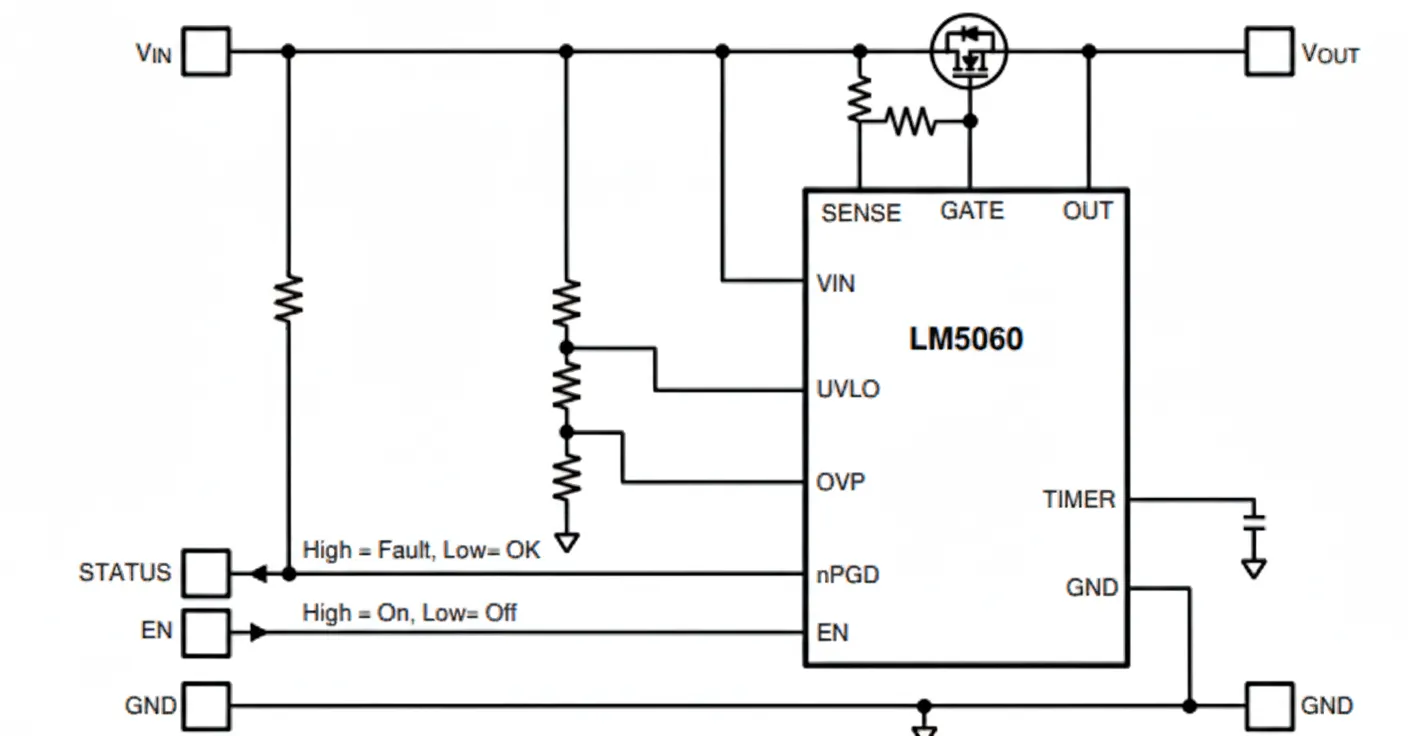
NMOS charge pump high-side driver IC examples
On some vendors' product pages, high-side MOSFET drivers are not always cataloged separately; they are sometimes listed under hot-swap controllers which integrate additional current limiting and differential amplifier features for surge protection. For example, some TI high-side switch products integrate MOSFETs and cannot drive external MOSFETs. ADI and other vendors offer hot-swap controllers and high-side gate drivers that can drive external MOSFETs; example parts include LTC4380, ADM4210, LTC4440, LTC7000.
With increased adoption of FOC motor control, integrated MOSFET driver ICs that combine three-phase half-bridge drivers with DC-DC regulation, charge-pump trickle charging, programmable amplifiers, and configurable dead-time control (for example DRV8301, DRV8305) are increasingly used in product designs.
3. PMOS High-Side Power Switch
(High-side drive; stable and simple)
NMOS high-side switching may offer better performance, but it requires additional gate-driver circuitry which increases complexity and cost. Outside of motor control and power conversion, where very low on-resistance, fast switching, or high current handling are required, PMOS is often the simpler and lower-cost choice for a high-side switch.
Although PMOS performance historically lags NMOS, process improvements have produced PMOS devices with Rds(on) < 10 mΩ in some cases. The main advantage of PMOS for high-side switching is that it does not require a charge pump, making the circuit simpler and cheaper.
Basic PMOS high-side switch behavior: CONTROL is a signal in the range 0...VCC. When CONTROL = 0 V, Vgs = 0 - VCC = -VCC, so the PMOS turns on and the load operates. When CONTROL = VCC, Vgs = 0 and the PMOS turns off.
Note that CONTROL low must be sufficient to produce a Vgs magnitude that turns the PMOS fully on, while Vgs must remain within the device's specified limits to avoid damage. Since MCU I/O levels are typically fixed at 3.3 V or 5 V while VCC may vary widely, directly driving the PMOS from an MCU I/O can fail to fully turn the PMOS off or can expose the MCU I/O to voltages beyond its rating. To avoid this, a small NMOS or NPN transistor is often used as a level shifter to drive the PMOS gate.
Example: an NMOS Q3 is used to shift the control level and drive PMOS Q2. When CONTROL = 0, Q3 is off and Q2 gate is pulled up to VCC so Q2 is off. When CONTROL = 1, Q3 conducts and pulls Q2 gate toward ground so Q2 Vgs is negative enough to turn Q2 on and the load operates.
If VCC is high, the PMOS Vgs during on-state can exceed the device's Vgs rating and damage the PMOS gate. To prevent gate overvoltage, add a zener diode and resistor to clamp Vgs so it does not exceed the PMOS rating (for example clamping to about -12 V). When VCC is high, recalculate resistor power dissipation and select appropriate component power ratings or alternate resistor values.
Using PMOS as a low-side switch is uncommon and generally not advantageous. Low-side switching is almost always implemented with NMOS due to better performance and simpler design.