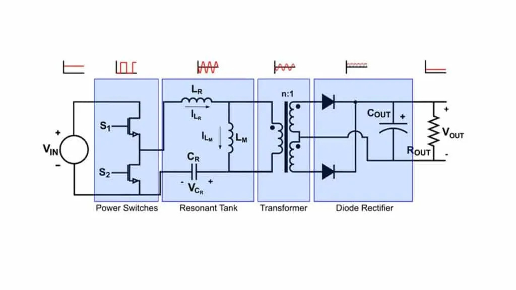
Overview
In DC-DC power circuits, PCB layout is critical to achieving circuit functionality and meeting performance targets. This article uses a buck converter as an example to summarize practical PCB layout approaches and design considerations.
Power-loop and current paths
Using the simplest buck topology as an example, the current paths when the high-side switch is on and off define the power loop. This part of the circuit supplies the load and carries significant power.
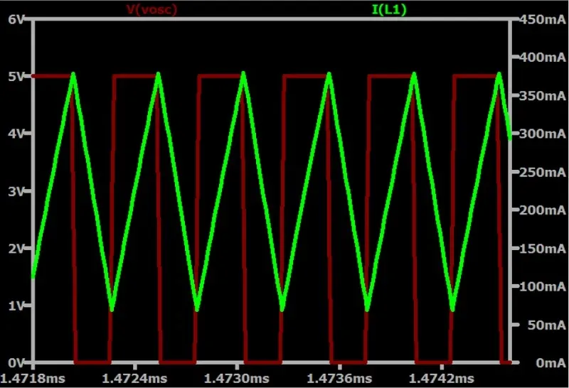
From the switch current waveforms it is clear that, due to the inductor, most of the circuit does not experience rapid current changes; the high di/dt occurs only in the switch nodes. During PCB routing, minimize the area of these fast-changing loops to reduce interference to other circuits. With modern integration, many power ICs now integrate the high- and low-side switches on-chip.
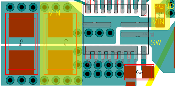
Example: MPQ8633A(B) power-loop layout
As an example, the MPQ8633A(B) series is a fully integrated high-frequency synchronous buck converter capable of 12–20 A output. The power-loop (green) contains input capacitors, the inductor, and output capacitors.
Recommended PCB layout principles
Keep the power loop area as small as possible to reduce emissions and parasitic elements. Key points:
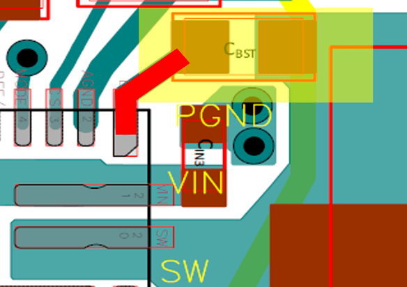
- Place input capacitors close to the chip VIN pin and power ground (PGND) to minimize parasitic inductance. Because input current is discontinuous, parasitic inductance can generate noise that affects the IC's voltage withstand and logic. Place at least one decoupling capacitor adjacent to each VIN pin to filter AC noise from the supply and any back-injected noise; spacing between the capacitor and pin should be less than 40 mil.
- Make power-loop traces short and wide to keep loop area small and reduce radiated noise.
- The SW node is a primary noise source; keep its high-current loop area as small as possible and keep it away from sensitive nodes such as FB.
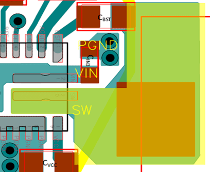
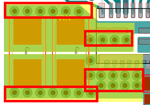
- Copper pour area and via count affect current capacity and thermal performance. PCB current capacity depends on board material, thickness, trace dimensions, and temperature rise; refer to IPC-2152 for accurate calculations. For the MPQ8633A(B) PCB, use multiple vias at VIN (at least 6) and PGND (at least 9) and maximize copper in these areas to reduce parasitic impedance. Widen copper at the SW node to avoid inadvertent current limitation.
Control and signal-layout considerations
Layout of the IC's control and reference circuits also requires careful attention.
Combine the following layout practices:
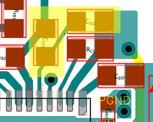
- Place the bootstrap (BST) capacitor as close as possible to the BST and SW pins. Use a route width of 20 mil or wider for the connection.
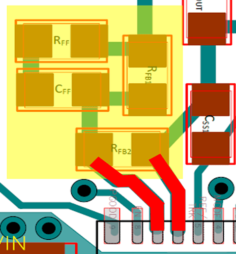
- Keep the feedback (FB) resistor network connection to the FB pin as short as possible to reduce noise coupling. The FB node is the most sensitive and a common cause of system instability. Keep it away from noise sources such as the SW node, inductor, and diodes. Place components like RFF, CFF, RFB1, and RFB2 close to the IC.
- Place the VCC decoupling capacitor close between the VCC pin and signal ground (AGND), preferably on the same layer without vias. For ICs with a combined AGND/PGND pin, connect the capacitor close to that pin.
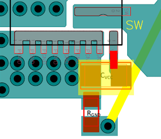
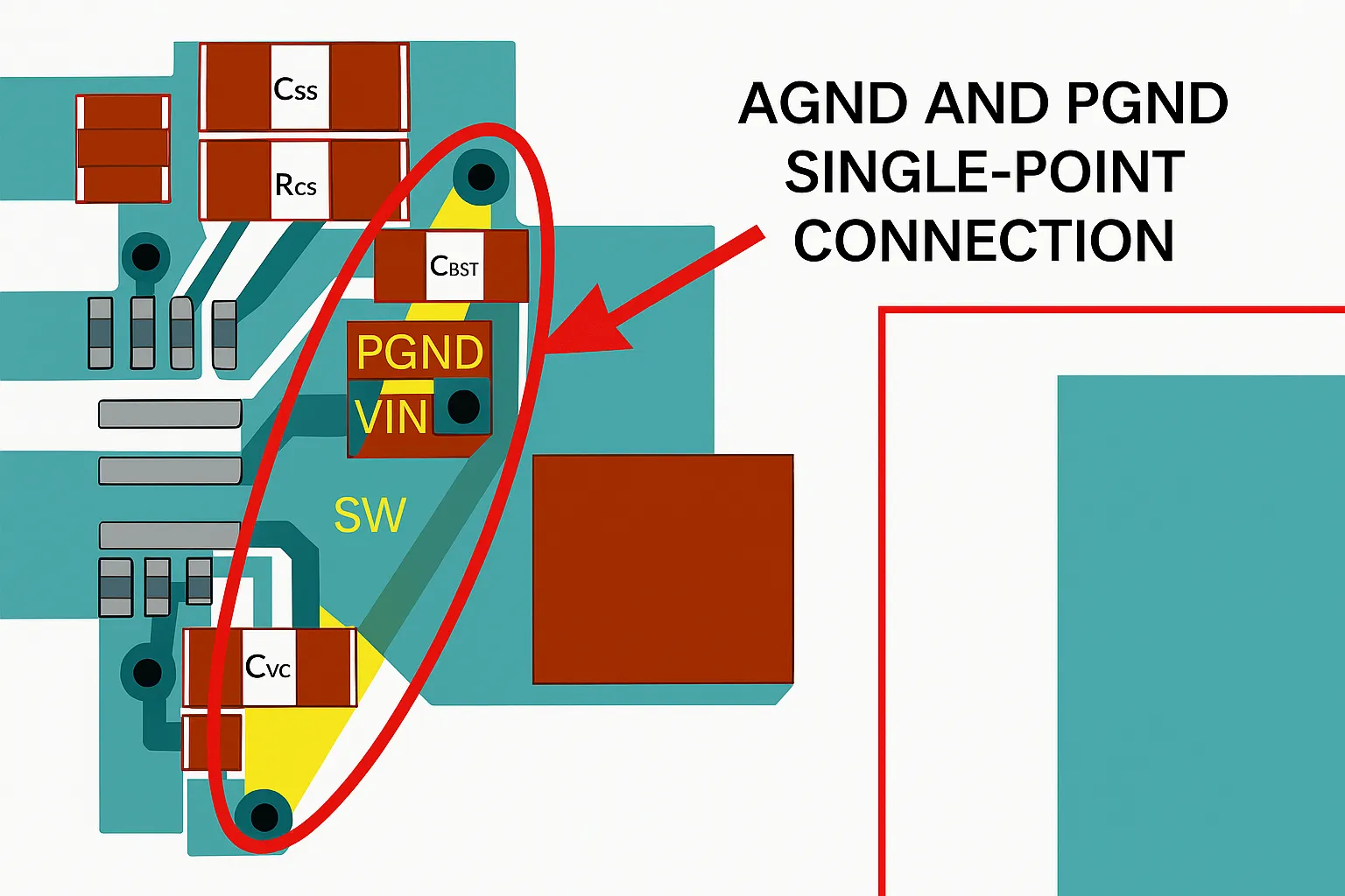
- Connect AGND and PGND at a single point (single-point connection).
- Place the soft-start (SS) capacitor close to TRK/REF and RGND.
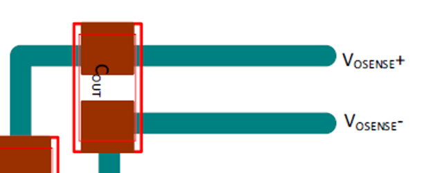
- Place the SENSE capacitor between the output sense traces and route it in parallel with the sense line.
- Avoid 90-degree trace corners for routing and copper pours; use 45-degree angles or arcs, especially on high-frequency traces, to reduce reflections and signal distortion.

Design checklist
For a quick assessment of whether a PCB layout is reasonable, the following reference images provide a simple self-check guide for basic buck and boost designs. Single-layer or two-layer boards are often sufficient for simple converters. The checklist is for reference only.