In modern electronics, reliable power delivery forms the foundation of system performance. From industrial control and new energy applications to automotive, telecom, and consumer devices, power integrity directly impacts signal quality, thermal behavior, EMI/EMC compliance, and long-term reliability. At Aivon, we specialize in PCB manufacturing that supports these demanding power applications through optimized stack-ups, material selection, thermal management, and precise fabrication processes.
This article consolidates key concepts in protective earthing, neutral conductors, instrument transformers, buck-boost configurations, linear regulators, LDOs, and DC-DC converters, reframed through a PCB engineering lens.
Protective Earth vs. Neutral: Critical Safety Distinctions in PCB Power Design
Protective Earth (PE) and Neutral (N) serve fundamentally different roles and must never be interchanged in PCB-based systems.
- Protective Earth (PE): Provides a low-impedance safety path for fault currents. It connects equipment enclosures to true earth, enabling protective devices (fuses, breakers, RCDs) to operate quickly during insulation failure. PE remains at near-zero potential relative to local earth.
- Neutral (N): Acts as the return path for normal load current in AC systems. It carries unbalanced current in three-phase setups and is grounded at the distribution transformer or substation, but it can develop voltage offset due to line impedance or faults.
Key differences relevant to PCB design:
- PE must never carry normal operating current; Neutral does.
- Swapping or combining them can energize chassis or PCB grounds, creating shock hazards and violating safety standards.
- In PCB layout, PE connections influence chassis grounding, shield ties, and isolated vs. non-isolated power domains.
Identification best practices:
- Color coding: PE typically yellow/green, Neutral blue/black.
- Testing: Multimeter resistance to earth, voltage measurements, or RCD-based methods. Always follow local codes.
Merging Neutral and PE on a PCB (e.g., in improper single-point grounding) risks ground loops, noise injection into analog/digital sections, and safety failures. High-reliability designs separate them clearly with dedicated planes or traces.
Why Grounding Resistance Matters: Targeting <= 4 ohms for Safety and Performance
Ground resistance directly affects fault current magnitude and touch/step voltages. Standards often limit protective/safety grounding to <= 4 ohms to keep fault voltages below safe thresholds (typically < 50V AC).
Why 4 ohms?
For typical fault currents (~10A), a 4 ohms resistance produces ~40V drop - within safe limits per empirical safety data.
Lower resistance improves discharge efficiency for lightning, static, and fault currents.
PCB design implications:
- Chassis and system grounding: Use thick copper pours, multiple vias, and strategic via stitching for low-impedance paths.
- Material and stack-up: High-Tg FR4 or metal-core PCBs for thermal dissipation in high-current grounding areas. Copper thickness (2oz+) reduces resistance.
- Layout techniques: Single-point grounding for low-frequency analog sections; multi-point for high-frequency digital/RF to minimize loops. Separate analog, digital, power, and chassis grounds, tying them at one low-impedance point.
In new energy and industrial PCBs, inadequate grounding leads to EMI issues, signal integrity degradation, and reliability failures under environmental stress.
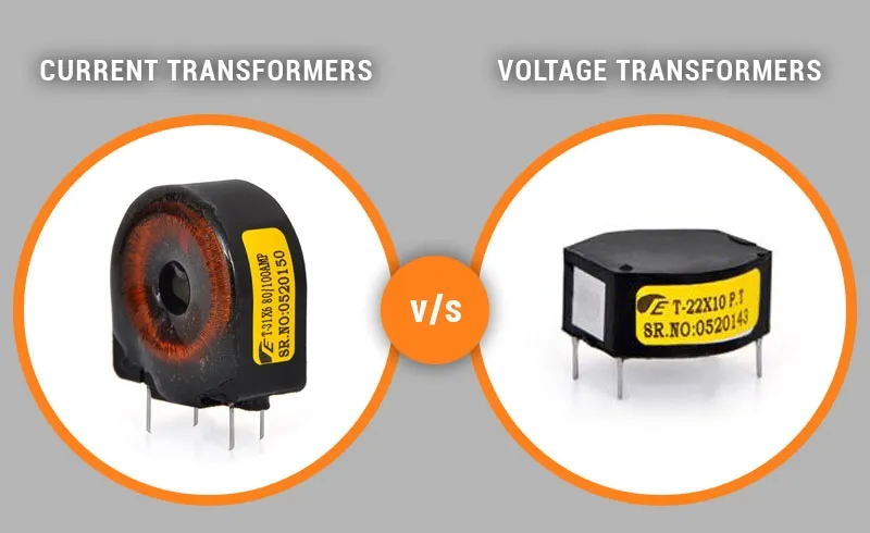
Current and Voltage Transformers: PCB Integration for Measurement and Protection
Current Transformers (CTs): Step down high primary currents for safe measurement and protection. Primary in series with load; secondary to meters/relays.
Voltage Transformers (VTs/PTs): Step down high voltages for parallel connection to monitoring circuits.
Key differences:
- CTs handle current scaling with low secondary burden; risk of open-secondary high voltage.
- VTs handle voltage scaling; primary high turns count.
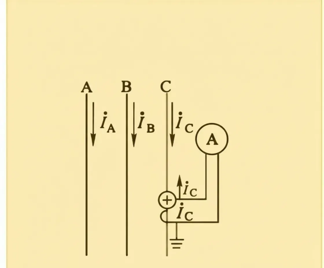
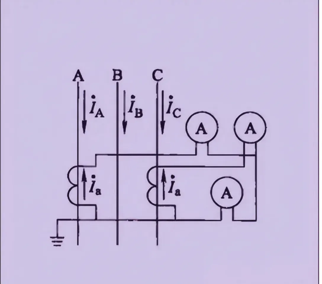
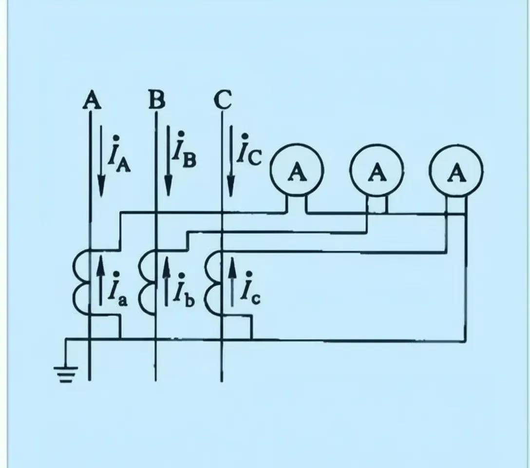
Common CT wiring configurations (critical for PCB relay/protection circuits):
- Single CT: Single-phase measurement.
- Two CTs incomplete star or differential: Phase-to-phase protection.
- Three CTs star/delta: Comprehensive three-phase protection.
- Zero-sequence: Ground fault detection.
PCB considerations:
- Isolation, creepage, and clearance per safety standards (material selection, slotting).
- Trace routing for low-burden secondaries to minimize errors.
- Shielding and grounding to reduce noise coupling into sensitive analog sections.
- High-current primary paths require heavy copper and thermal vias.
Buck-Boost Transformers: Voltage Correction in Power PCBs
Buck-boost transformers correct line voltage sags or mismatches (e.g., 208V to 230V systems) via autotransformer configurations.
Applications:
- Motor starting, heater elements, industrial equipment.
- Series/parallel secondary wiring adjusts boost amount.
PCB-level impact:
- Downstream DC-DC or linear regulators see more stable input, improving efficiency and ripple performance.
- Power distribution layers must handle corrected higher currents/voltages with appropriate copper weight and thermal design.
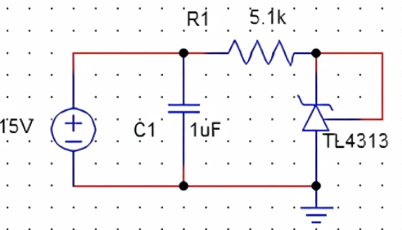
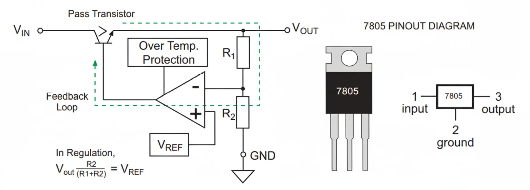
Linear Regulators, LDOs, and DC-DC Converters: Power Delivery on PCBs
Linear Regulators: Dissipate excess voltage as heat. Simple, low-noise, but efficiency drops with large Vin-Vout differentials.
LDOs: Low-dropout variants using P-channel MOSFETs enable tighter margins (100mV dropout common). Excellent for noise-sensitive rails (analog, RF, sensors).
DC-DC Converters (switching): High efficiency (90%+), handle wide Vin-Vout, but introduce switching noise and require careful inductor/capacitor selection.
Design trade-offs and tips:
- Use LDOs for low-noise post-regulation after switching stages.
- High-current linear designs (e.g., LT1083 family) need robust thermal planes, vias, and heatsinking on PCB.
- Layout: Minimize high di/dt loop areas, use ground planes, multiple decoupling caps across frequency ranges, short switch-node traces.
- PSRR (Power Supply Rejection Ratio): Critical metric. Measure by injecting AC ripple and comparing input/output. High PSRR LDOs essential for clean analog supplies. PCB layout (bypass caps, plane integrity) heavily influences real-world PSRR.
PCB Manufacturing Considerations for Robust Power Systems
Successful power electronics demand close collaboration between design and fabrication:
- Stack-up optimization: Multiple ground planes, thick copper for power, controlled impedance where needed.
- Thermal management: Copper pours, thermal vias, metal core or high-Tg materials for regulators and high-current paths.
- Reliability: Proper clearances/creepage for safety isolation, solder mask quality, via filling for high-current.
- EMI/EMC: Grounding strategy, shielding, component placement to reduce loops and radiation.
- Material selection: FR4 variants, Rogers for RF/power, based on thermal, dielectric, and mechanical needs.
At Aivon, our advanced PCB capabilities ensure these power designs translate into reliable, high-performance boards across new energy, industrial, automotive, and other sectors.
Conclusion
Understanding protective earthing, neutral handling, transformers, and modern regulation topologies is essential for any high-reliability PCB project. By centering these elements in layout, material choice, and manufacturing, engineers achieve better signal integrity, thermal performance, safety compliance, and overall system robustness. For complex power PCB requirements, partnering with an experienced manufacturer like Aivon helps bridge design intent with production excellence.