This article introduces ideal and practical circuit simulation methods, reviews switching waveforms, examines PCB layout, and uses ideal simulation models to confirm which components are suitable when a regulator operates at high switching frequency.
Part 01: Set inductor and output capacitor constants
DC/DC converters typically switch between 300 and 500 kHz, but products with switching frequencies of 1 to 2 MHz are becoming more common, and some reach 4 MHz or higher. High-frequency DC/DC converters allow reductions in the size of output capacitors and inductors to save PCB space, which is important for compact portable designs, but achieving low output voltage at higher switching frequencies can be more challenging.
Here we use an ideal boost-converter circuit in LTspice to validate the design. The circuit in Figure 1 uses VIN = 6 V, VOUT = 12 V, and load current = 10 A. We compare the required inductance and output capacitance for switching frequencies of 2 MHz and 400 kHz and then verify whether the circuit preserves the same characteristics when the calculated component values are applied.
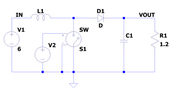
Figure 1 Boost converter circuit
Part 02: Choosing the inductor
Before calculating inductance, compute the duty ratio using the formula in Figure 2, where Vo is the output voltage, VIN is the input voltage, and VD is the diode forward drop.
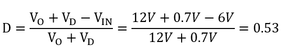
Figure 2 Duty ratio formula
Next, calculate the inductance for 2 MHz (L1) and 400 kHz (L2) using the formula in Figure 3, where ΔIL is taken as 40% of the load current. At 2 MHz the inductance is roughly one fifth of the value at 400 kHz, so the number of turns is reduced and a smaller inductor package can be selected. This shows that a primary advantage of higher switching frequency is that smaller inductor packages are feasible.
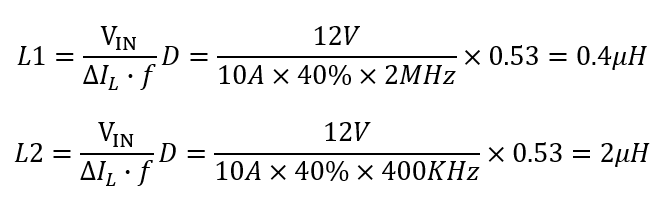
Figure 3 Inductor calculation formula
Part 03: Choosing the output capacitor
Use the formula in Figure 4 to calculate the output capacitor. Here ESR is the capacitor ESR, and the required capacitance is determined by the acceptable output ripple.
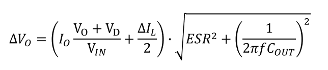
Figure 4 Output ripple voltage formula
For an idealized case with ESR = 0, the formula simplifies to the expression shown in Figure 5, which gives the required output capacitance.
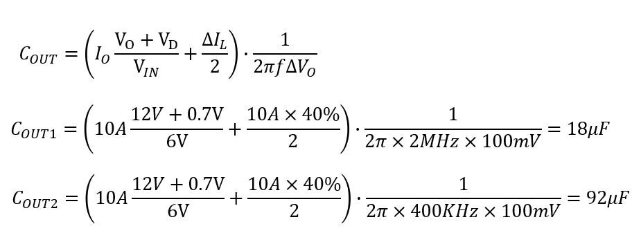
Figure 5 Output capacitor calculation formula
Using these formulas, the calculated output capacitances are Cout1 = 18 uF for 2 MHz and Cout2 = 92 uF for 400 kHz. Thus, higher switching frequency requires smaller output capacitance. The next step is to simulate and verify that the chosen inductors and output capacitors produce the desired output voltage.
Part 04: Verification with LTspice
We used LTspice to verify the ideal boost converter from Figure 1 with the calculated inductance and output capacitance at switching frequencies of 2 MHz and 400 kHz, checking that the circuit delivers 12 V output with comparable ripple.
Figure 6 Boost regulator schematic for 2 MHz and 400 kHz
Figure 7 shows the simulated output voltages. The red trace (Vout1) is for 2 MHz: about 12 V with ripple near 149 mV. The blue trace (Vout2) is for 400 kHz: about 11.95 V with ripple near 145 mV. These results indicate that the selected inductors and output capacitors are acceptable, and that compact inductors and capacitors can be used with high switching-frequency regulators.
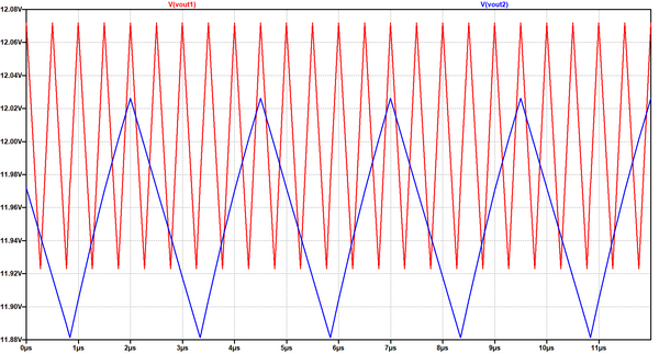
Figure 7 Output voltage waveform
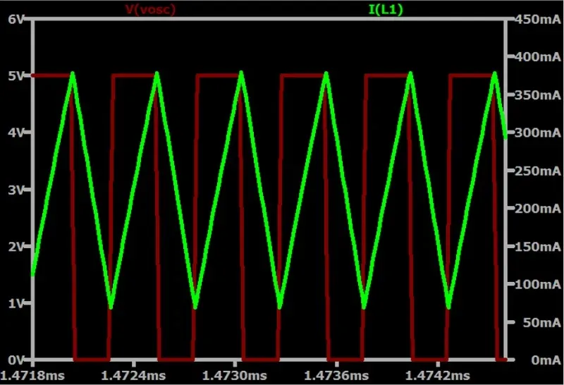
However, examine the current waveforms in Figure 8. The blue inductor current has a low slew rate and is amenable to filtering by the input capacitor. The currents through the switch (red) and the output capacitor (green) are PWM currents with fast slew rates. PCB layout for these fast-slew currents must be carefully designed. In these simulations we used the same slew rate for 2 MHz and 400 kHz cases; in real hardware the slew rate at 400 kHz may be faster than at 2 MHz depending on the switching device and circuit parasitics.
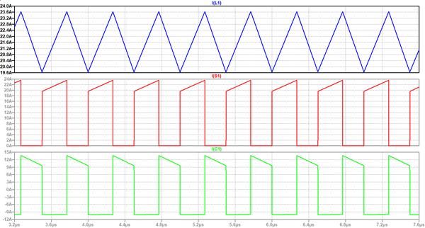
Figure 8 Current waveforms
Part 05: Summary
Simulation shows that higher switching frequency reduces the size of inductors and capacitors used in a regulator. However, higher frequency also brings challenges: increased switching losses, higher switching node slew rates, and higher current slew rates, and it can be difficult to find suitable MOSFETs. MOSFETs must have sufficiently low Rds(on) to minimize conduction loss and support fast switching. Component placement and routing should minimize PCB parasitic inductance, and sensitive nodes must be protected from noise propagation.