Peak detector overview
A peak detector extracts the peak of an input signal and produces an output Vo = Vpeak. To achieve this, the circuit holds the output until a new larger peak appears or the circuit is reset.
Peak detectors are widely used in AGC (automatic gain control) circuits and in sensor peak-value extraction circuits, and are often used as the criterion for selecting the gain setting of programmable gain amplifiers. Some designers prefer using RMS chips such as the AD637 because of integration convenience, but that approach is not always appropriate: the RMS value does not necessarily correspond to signal positive and negative peaks, and such chips are costly in practical applications. They may be acceptable in competition settings where test signals are sine or square waves.
AC versus DC measurement considerations
A steady DC voltage has a single relevant property: its magnitude. In contrast, an AC supply has frequency, peak voltage, and RMS value. Therefore when working with AC voltages, it is usually necessary to measure frequency, peak, and RMS. This article focuses on peak voltage detection circuits.
A reliable power converter must provide overvoltage and undervoltage protection. For DC voltages, this can be implemented by dividing the voltage with resistors and feeding the result into a hysteresis comparator.
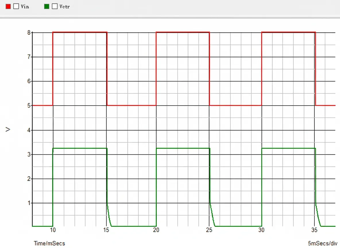
Approach for AC over/under voltage protection
For AC, overvoltage and undervoltage protection is more complex. It requires detecting the peak voltage and holding that detected peak for a certain time. A straightforward approach is to full-wave rectify, then divide and filter.
Simulation and observed timing error
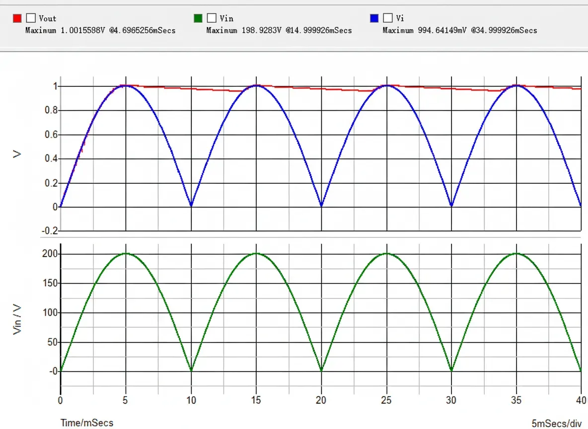
From the simulated circuit above, the divider ratio is 1 kΩ/(199 kΩ + 1 kΩ) = 0.005, so the detector output should be 200 V × 0.005 = 1 V. However, the simulation result is about 0.6 V, as shown below.
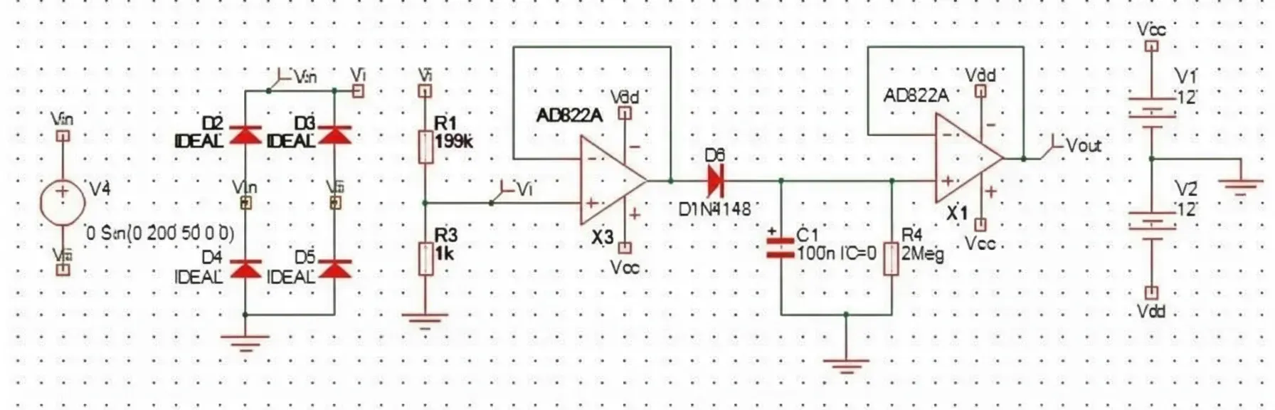
The simulation shows that the output voltage Vout lags the pre-filter voltage Vise, so when Vise reaches its peak the filter capacitor C1 only charges to 0.6 V. This voltage depends on the resistor divider and the filter capacitance, so the desired voltage cannot be obtained simply from the divider ratio, making early design calculations inaccurate.
Phase-lag compensation method
A small modification to the circuit can compensate this phase lag so that the held output matches the divider calculation at peak. After the modification, the simulation shows the output voltage consistent with the divider-based design.
Concluding question
The simulation shows that the output now matches the divider calculation. How does this compensate the phase lag?