Overview
In switching power supplies there are the usual differential-mode and common-mode noise sources, but other high-frequency noise sources can also cause electromagnetic compatibility (EMC) problems. Two common high-frequency oscillation sources are: high-frequency oscillation caused by MOSFET switching transitions, and oscillation caused by rectifier diode reverse recovery. These oscillations can be mitigated by appropriate snubber (absorption) circuits.
Effect on signal spectrum
High-frequency ringing and overshoot significantly increase a signal's high-frequency harmonic content. The result is more high-frequency noise that is likely to create EMC issues.
1. Oscillation from the switching transistor
Using a flyback power supply as an example, ideally the MOSFET drain/source waveform is a trapezoid determined by switching. In practice, transformer primary leakage inductance and parasitic capacitance between the MOSFET drain and source form an LC tank. When the MOSFET abruptly switches off, this LC network rings and introduces high-frequency oscillation.
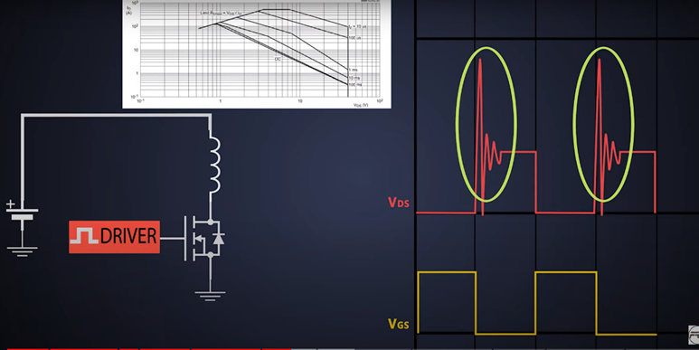
Figure: MOSFET waveform in flyback power supply
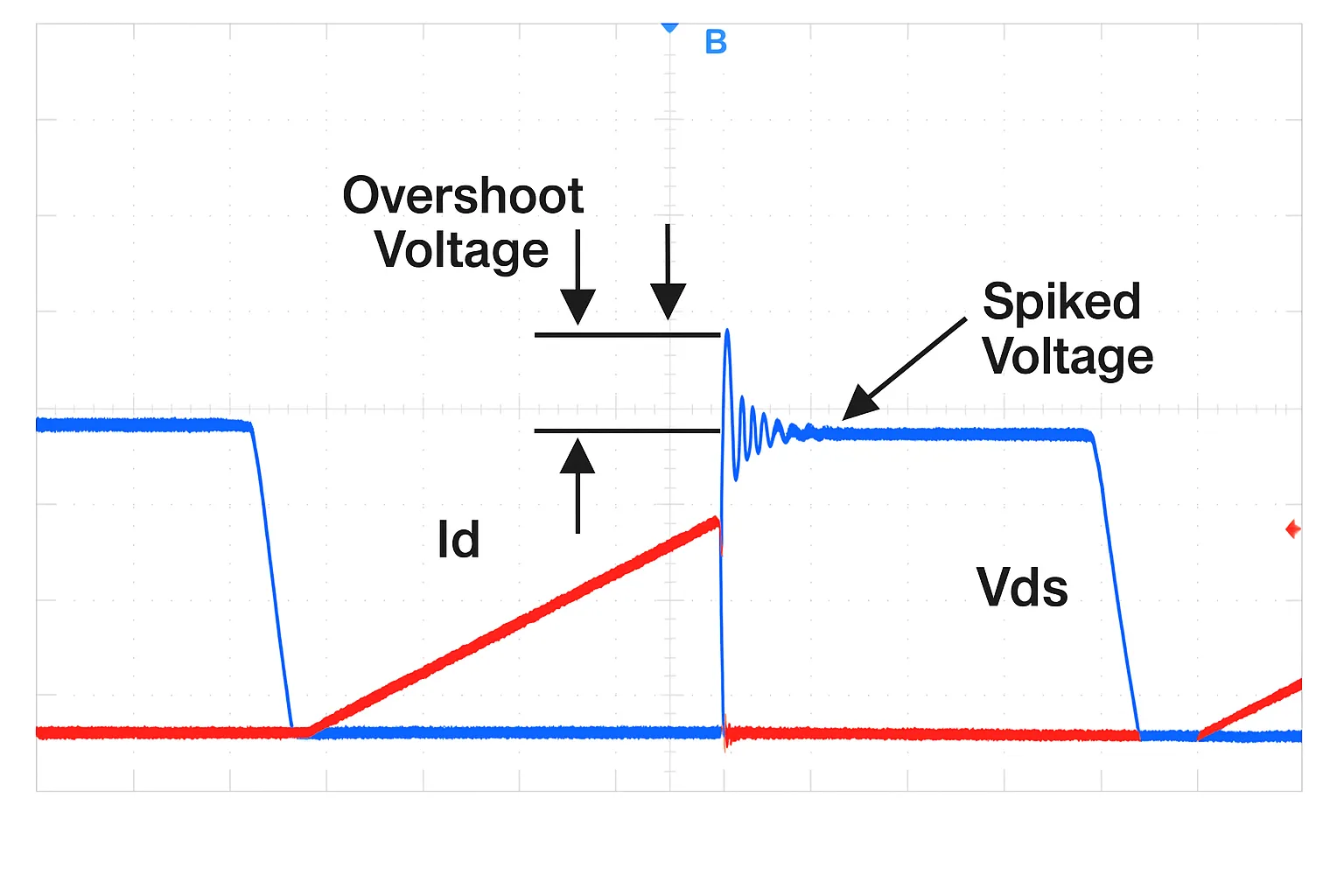
Figure: Voltage and current waveforms across MOSFET drain-source
The large dv/dt across the MOSFET is a source of common-mode noise. Ringing increases the high-frequency content of this voltage. To reduce this ringing, design a snubber network to absorb the energy in the LC loop.
RCD snubber variants for flyback
Two common RCD snubber configurations used with flyback converters are shown below. With reasonable component selection, the snubber resistor and capacitor dissipate and absorb the ringing energy, reducing the high-frequency components on the MOSFET waveform. For detailed RC design procedures, consult technical literature on RCD snubbers for switching power supplies.
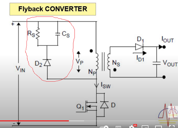
Figure: Flyback RCD snubber, variant 1
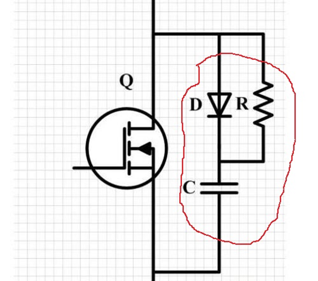
Figure: Flyback RCD snubber, variant 2
2. Oscillation from rectifier diode reverse recovery
Rectifier diodes exhibit reverse-recovery current spikes that can cause significant ringing. These oscillations become high-frequency differential-mode noise. The noise can appear on the secondary output and can couple through the transformer to the primary, adding to overall interference.
Placing an RC snubber in parallel with the diode effectively reduces high-frequency noise. The snubber confines the high-frequency ringing to a small local loop that includes the diode and the R-C network, minimizing the impact on the rest of the circuit. Because high-frequency currents flow in the RCD loop, keep this loop area as small as possible to limit radiated emissions. Typical RC values are 470 pF and 10 ohms.
Another approach is to place a ferrite bead in series with each rectifier diode to increase high-frequency impedance and reduce ringing amplitude. Combining ferrite beads with RCD snubbers is often the most effective solution.
Because secondary rectifiers operate at much higher current levels than primary rectifiers, secondary diode reverse-recovery is typically the dominant source of this type of interference.
Practical considerations
When implementing snubbers, minimize loop area and place components close to the switching device or diode being protected. Balance snubber sizing: an overly large snubber can increase steady-state losses, while an undersized snubber may not sufficiently suppress ringing. Combine snubbers with layout techniques and ferrite beads for best EMI performance.