In circuit design, especially for active circuits such as power amplifier bias networks, fan-shaped microstrip lines are commonly used in bias circuits. This approach is typical in power amplifier designs because it involves controlling the gate bias voltage (Vg) and drain bias voltage (Vd) of the amplifier device. In these designs, RF signals must be fully isolated from the bias voltages to ensure correct circuit operation.
Principle and Role of Fan-shaped Microstrip
To isolate RF signals, quarter-wavelength microstrip stubs are commonly used. For RF, a short at the stub end is transformed into an open at the feed when using a quarter-wavelength transmission line, providing RF isolation. However, additional measures are sometimes required to ensure DC signals are not affected by RF, which is where the fan-shaped microstrip comes into play. The fan-shaped microstrip acts like a bypass capacitor in an active bias network, separating RF and DC so that RF does not disturb the DC bias source. Typically, the radius of the fan-shaped microstrip is chosen to be one quarter wavelength, making its arc length equivalent to a quarter wavelength. The angular span is often around 90 degrees to ensure effective RF isolation. In practical designs, the open-circuit fan-shaped microstrip must be designed carefully. From the bias port perspective the RF appears as a short, so after the quarter-wave transformation the bias sees an open, achieving effective RF/DC isolation.
The following reproduces an experiment from a CSDN blog by the user "怡步晓心l".
1. Design Requirements
The example designs an F-class amplifier bias network. The requirements are that the fundamental and odd harmonics appear as open circuits to ground, while even harmonics are shorted to ground. In general, an F-class amplifier bias network can also be applied to generic power amplifier bias circuits. The specific requirements are:
- Center frequency: 2.4 GHz
- Fundamental to ground open: fundamental-to-ground impedance > 10000 ohm
- Second harmonic to ground short: second-harmonic-to-ground impedance < 1 ohm
- Third harmonic approximately open: third-harmonic-to-ground impedance > 200 ohm
- Do not affect the pass of the fundamental
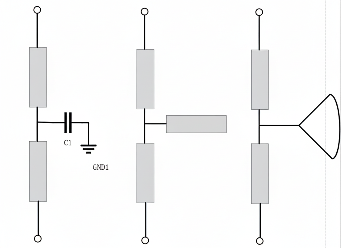
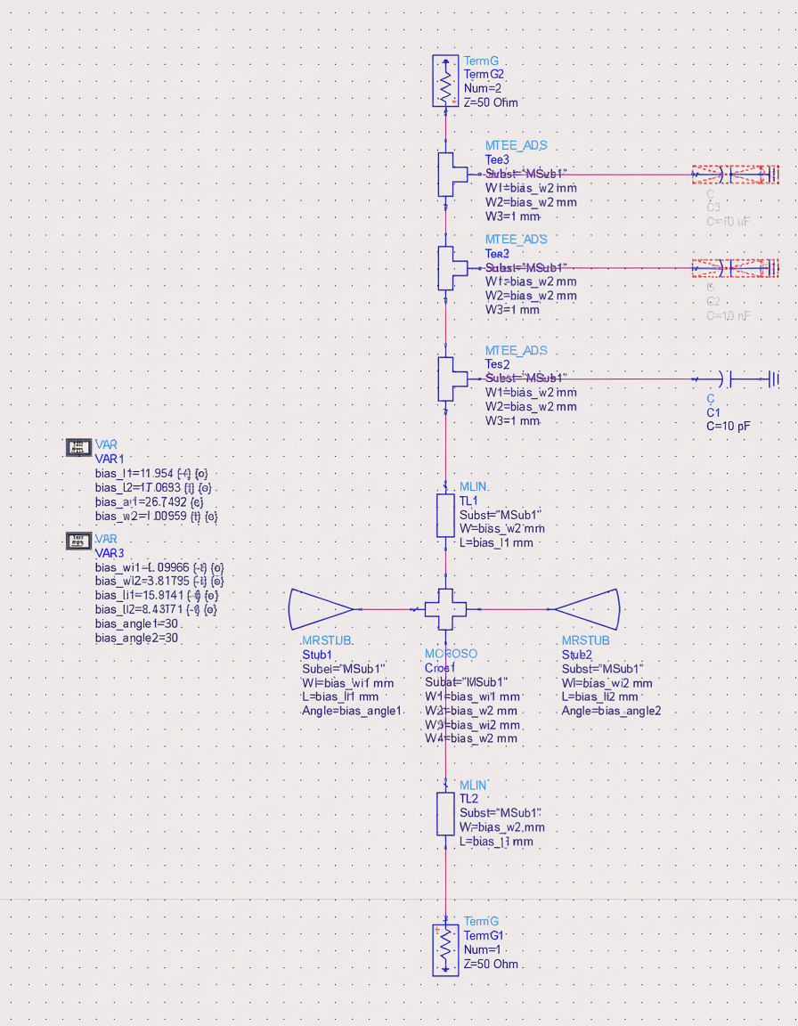
2. Schematic Design
The schematic follows the theoretical topology. TL2 is a quarter-wavelength line, and the two fan-shaped microstrip stubs operate at the fundamental and second-harmonic frequencies, respectively. This makes port 1 see the fundamental and third harmonic as open to ground, while the second harmonic is shorted to ground. The schematic is simulated and tuned to obtain the following result.
Simulation of the schematic shows that the design can basically meet the requirements. The next step is layout-level EM simulation.
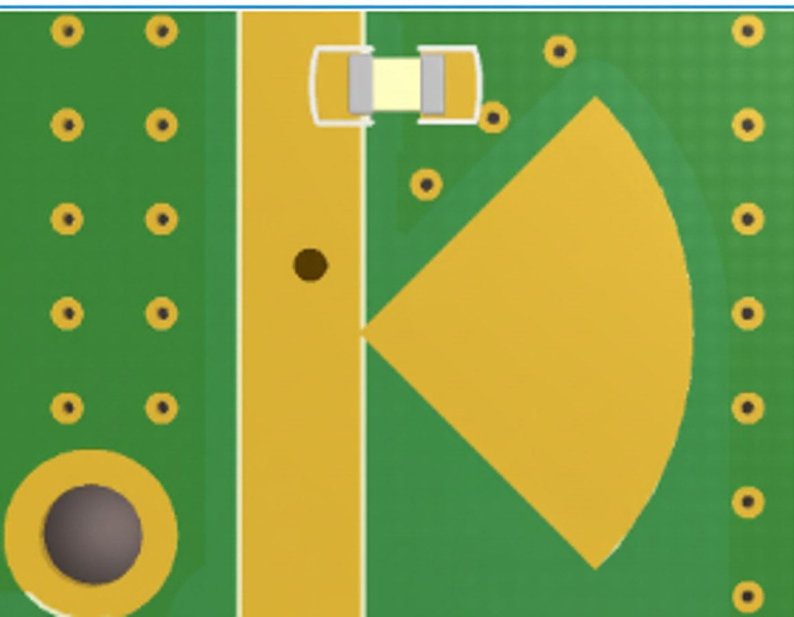
3. Layout EM Simulation
For the layout EM simulation, a Rogers 4350B substrate is used with parameters 3.66 and 0.0037. The substrate and ports are set up appropriately and the layout is generated as shown below.
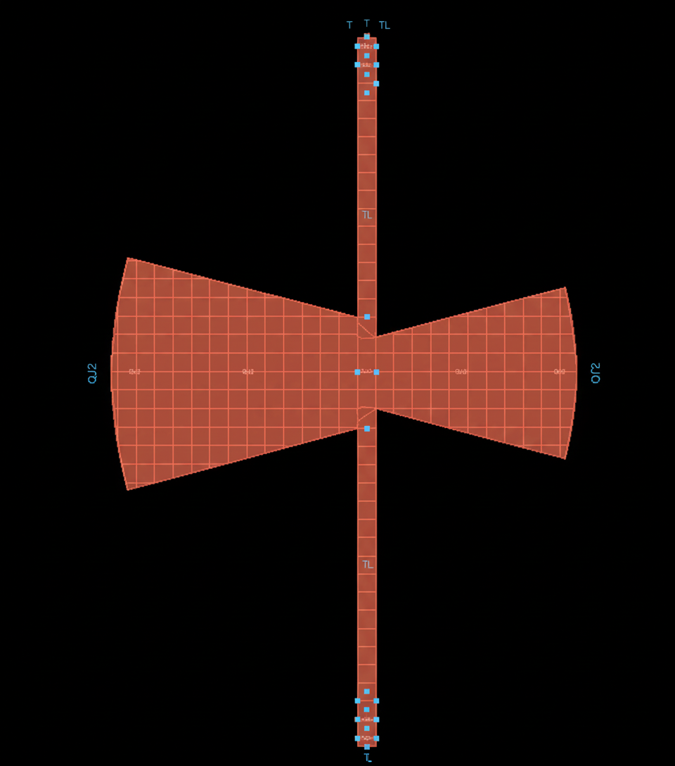
The layout is configured with layout parameters and details not repeated here. After all settings are applied, the layout EM simulation is run and the EM model is produced.
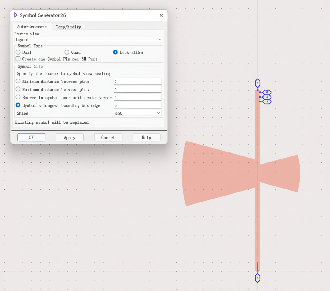
Using the layout, a symbol is created with the "looklike" option and appears as follows.
4. Layout Co-simulation
A new schematic is created for combined schematic/layout simulation, inserting the previously created symbol and related components.
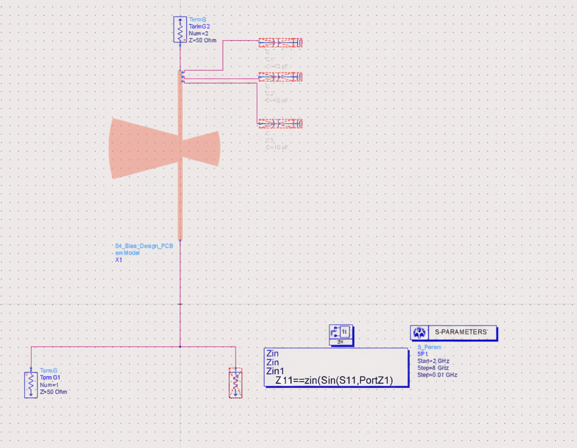
The EM model is selected as the simulation data source, and the frequency sweep parameters are set. The simulation produces the following result.
The bias network performs well and meets the requirements, but schematic-level and layout-level simulation results often differ and require fine tuning. For example, if the layout simulation center frequency shifts by 100 MHz to 2.5 GHz, the schematic-level design may need to be adjusted to 2.3 GHz so that the layout simulation is more likely to yield the target 2.4 GHz result.