Introduction
In surface mount technology (SMT) assembly, the stencil is a critical tool. It dictates the precise application of solder paste onto a printed circuit board. Its role in ensuring high yield and reliable solder joints cannot be overstated. This is especially true when dealing with a diverse range of component sizes for stencil. Achieving the correct solder paste volume for each component, from tiny 01005 chips to large QFNs or BGAs, hinges significantly on selecting the appropriate stencil thickness component size pairing. As an assembly engineer, I have seen firsthand how incorrect stencil specifications can lead to frustrating defects and costly rework. This detailed guide explores how to optimize your component stencil choices and design to prevent common issues and ensure robust SMT assembly.
What is a PCB Stencil and Why Thickness Matters
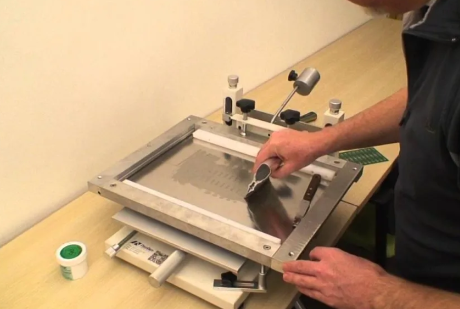
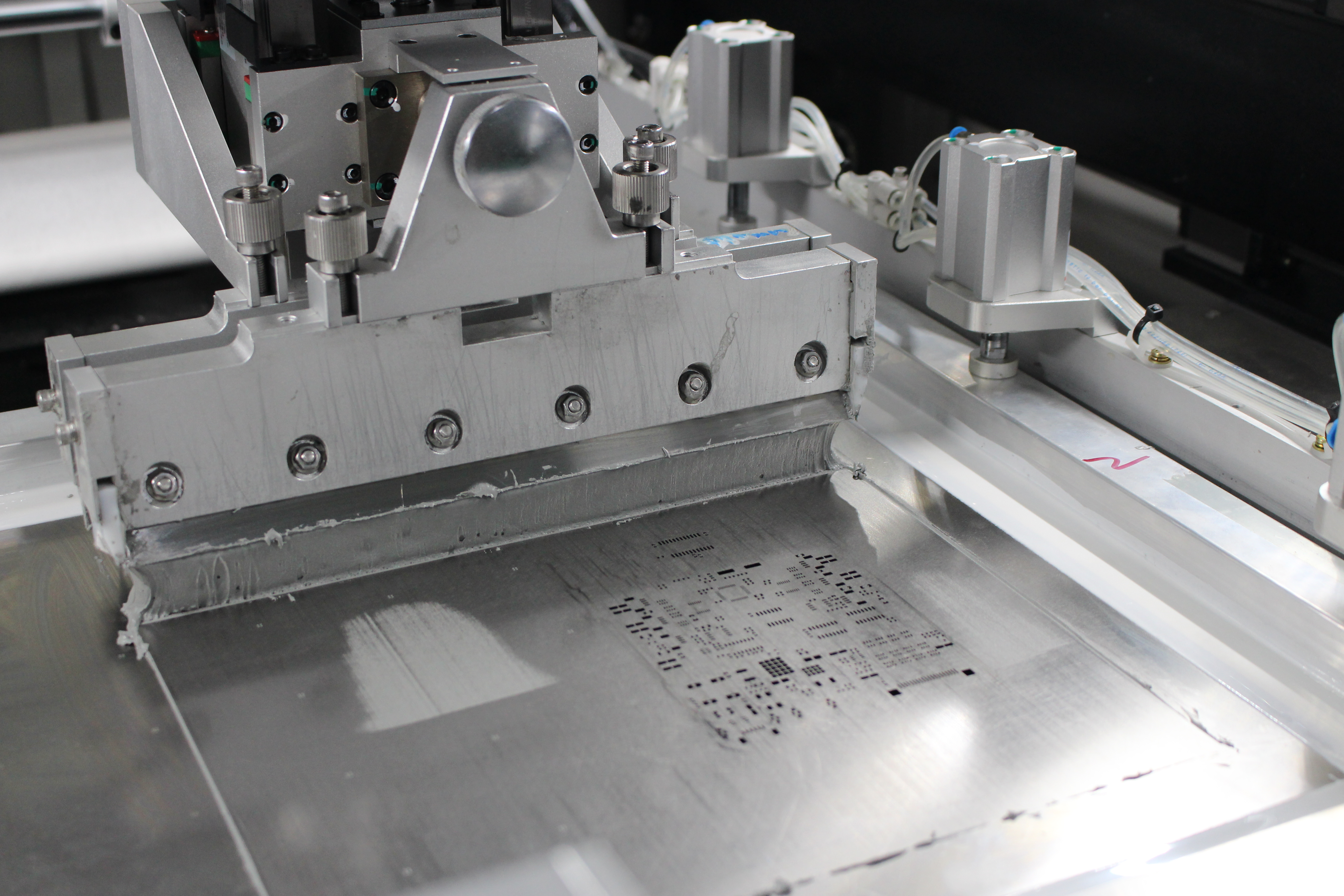
A PCB stencil is a thin sheet of material. It is typically stainless steel. This sheet has apertures (openings) precisely cut to match the pads on the PCB where components will be soldered. During the solder paste printing process, the stencil aligns accurately over the PCB. Solder paste is then applied across its top surface using a squeegee blade. The paste is forced through the apertures, depositing a controlled volume onto each corresponding pad.
The stencil thickness component size relationship is fundamental. The stencil's thickness, combined with the area of each aperture, directly determines the volume of solder paste deposited. If the stencil is too thin for a larger component, insufficient solder paste may result. This can lead to weak joints or opens. Conversely, if it is too thick for fine pitch components, excessive paste can cause bridging or shorts. Therefore, understanding this relationship is key to achieving optimal solder paste deposition for a mixed array of component sizes for stencil.
Related Reading: The Comprehensive Guide to SMT Stencil Engineering: From Design Optimization to Process Control
Factors Influencing Stencil Thickness Selection
Several critical factors influence the selection of the ideal stencil thickness component size for an assembly.
1. Smallest Component Pitch and Aperture Ratio
The pitch of the smallest component on the board is often the primary driver for initial stencil thickness selection.
- Aperture Ratio (Area Ratio): This is a key metric. It is defined as the area of the stencil aperture divided by the area of the aperture walls. IPC-7525A specifies that for good paste release, the area ratio should generally be greater than 0.66. If this ratio is too low, solder paste can stick to the stencil walls, resulting in insufficient deposit. For very fine pitch components, achieving this ratio often necessitates a thinner stencil.
- Aspect Ratio: This is the ratio of the aperture's width to the stencil thickness. For consistent paste release, the aspect ratio should typically be greater than 1.5. A lower aspect ratio can cause excessive solder paste to stick to the aperture wall during release. This means a thinner stencil is required for narrower apertures.
2. Component Types and Density
The mix of component types and their density across the board greatly influences stencil choice. A board primarily populated with large passive components might tolerate a thicker stencil. Conversely, a board with numerous fine pitch BGAs, QFNs, and 0.4 mm pitch ICs will demand a much finer approach. A PCB guide component analysis will identify the most challenging components in terms of paste volume requirements.
3. Solder Paste Type and Particle Size
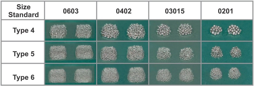
The rheology and particle size of the solder paste also play a role. Finer pitch components require solder paste with smaller particle sizes (e.g., Type 4 or Type 5). These pastes can release more easily from smaller apertures, sometimes allowing for slightly thicker stencils than would otherwise be possible.
4. Board Flatness and Pad Finish
Uneven board flatness can affect paste transfer efficiency, potentially requiring adjustments to stencil thickness or printer parameters. The pad finish also influences paste adhesion during printing.
Standard Stencil Thicknesses and Their Applications
Stencil manufacturers offer a range of standard thicknesses. Here is a practical overview of how they apply to various component sizes for stencil. Typical stencil thicknesses range from 0.08 mm to 0.15 mm (approximately 3 to 6 mils).
1. Thin Stencils (e.g., 3 mil / 75 µm to 4 mil / 100 µm)
- Application: These are typically used for boards dominated by very fine pitch devices. This includes components with pitches of 0.4 mm or less, such as many BGAs, QFNs, and smaller ICs. For extremely small components like 01005 (0.4 mm x 0.2 mm) or 0201 (0.6 mm x 0.3 mm), a 3 mil or even 2.5 mil (63.5 µm) stencil might be necessary to prevent bridging and ensure proper paste release from tiny apertures.
- Advantages: Excellent for preventing bridging on fine pitch pads.
- Disadvantages: May provide insufficient solder paste for larger components (e.g., large chip capacitors, power components). This potentially leads to opens or weak joints on those parts.
2. Medium Stencils (e.g., 5 mil / 125 µm)
- Application: This is a very common general purpose thickness. It suits boards with a moderate mix of component sizes, including 0.5 mm pitch devices, 0603, 0805, and 1206 passive components, and many standard SMT packages. It offers a good balance between paste volume for larger components and avoiding bridging on moderately fine pitch parts.
- Advantages: Versatile for a wide range of common components.
- Disadvantages: Might still struggle with the finest pitch devices (e.g., 0.4 mm pitch). It may also provide slight underfills for very large thermal pads without aperture modifications.
3. Thick Stencils (e.g., 6 mil / 150 µm to 8 mil / 200 µm+)
- Application: Used for boards primarily populated with larger components requiring substantial solder paste volume. This includes power components, larger SMT connectors, large chip components (e.g., 1210, 2512), and some through-hole components where paste-in-hole technology is used. It is also suitable for boards with limited fine pitch parts where higher paste volume is needed for robust joint formation. For BGAs with pitches greater than 1.0 mm, a 0.15 mm thickness is often selected.
- Advantages: Ensures strong, sufficient solder joints for large, high-power components.
- Disadvantages: High risk of bridging and solder balls when used with any fine pitch or small chip components.
Optimizing Stencil Thickness for Mixed Component Sizes
Most modern PCBs feature a diverse mix of component sizes for stencil, from ultra fine pitch to large power components. Simply choosing a single thickness often leads to compromises. Here are techniques to optimize paste volume across a heterogeneous board.
1. Step Stencils (Multi-Level Stencils)
This is a powerful technique for boards with significant variations in component sizes for stencil. Step stencils have varying thicknesses.
- Step-Down Stencil: For areas with very fine pitch components, the stencil material is made thinner than the main stencil thickness. This reduces the paste volume for these delicate components, preventing bridging.
- Step-Up Stencil: Conversely, for large components or thermal pads requiring more solder paste, the stencil is made thicker in specific areas. This ensures adequate paste volume for strong solder joints and efficient thermal transfer.
- Considerations: Step stencils add complexity and cost to stencil manufacturing. The step transition must be smooth to avoid squeegee damage and ensure consistent paste wiping. The stencil guide size for the step area is crucial. IPC-7525C provides guidelines for stencil design, including step stencils.
2. Aperture Design Adjustments
Even with a single stencil thickness, aperture modifications can fine tune solder paste volume.
- Aperture Reduction: For fine pitch components on a standard thickness stencil, reducing the aperture size (e.g., by 10-20% of the pad area, or shaping it as an "H" or "U") can decrease paste volume to mitigate bridging.
- Windowpaning/Multiple Openings: For large thermal pads (e.g., under QFNs, DFNs, BGAs), a single large aperture can lead to excessive paste and voiding. Instead, breaking the large aperture into multiple smaller openings (windowpaning) or a grid pattern helps control paste volume and reduces voids. This improves thermal performance and solder joint reliability.
- Home Plate/Rounded Corners: For specific leaded components like gull-wing leads, a "home plate" shape (a rectangular aperture with one side removed or rounded) can optimize paste deposition and reduce solder balls. Rounded corners on apertures also improve paste release.
3. Solder Paste Volume Calculation
Precise solder paste volume calculation is fundamental. The theoretical volume of solder paste can be calculated for each board. This ideal volume is typically determined by the component's lead dimensions and the desired solder joint height. Engineers often use a specific target volume for each component type. This guides the selection of stencil thickness component size and aperture modifications.
Related Reading: How Does Stencil Design Impact PCB Assembly Quality?
Troubleshooting Common Issues Related to Stencil Thickness
Incorrect stencil thickness component size selection and aperture design are root causes for many SMT defects.
- Insufficient Solder Paste (Opens, Cold Joints, Insufficient Fillets):
- Cause: Stencil too thin for component, aperture too small, or poor paste release from apertures (e.g., low aspect/area ratio). Stencil clogging or uneven pressure can also cause this.
- Solution: Increase stencil thickness (if possible without affecting fine pitch), enlarge aperture dimensions, or use a step-up stencil. Optimize paste release by improving aspect/area ratios (e.g., target aspect ratio > 1.5, area ratio > 0.66).
- Excessive Solder Paste (Bridging, Solder Balls, Shorts):
- Cause: Stencil too thick for component, aperture too large, or poor stencil guide size for step areas. Solder paste bridging typically occurs when paste connects two adjacent pads.
- Solution: Decrease stencil thickness (if possible), reduce aperture dimensions (e.g., by using aperture reduction or windowpaning), or use a step-down stencil.
- Solder Paste Smearing:
- Cause: Stencil not cleanly separated from the PCB, often due to improper squeegee pressure or speed, or an unclean stencil bottom. While not directly related to thickness, it affects deposit quality.
- Solution: Adjust printing parameters, ensure proper stencil cleaning cycles, and verify stencil alignment.
Conclusion
Mastering PCB stencil thickness for different component sizes is a cornerstone of achieving high yield and reliable electronic assemblies. The choice of component stencil thickness must be meticulously aligned with the smallest critical pitch on the board, while simultaneously accommodating the larger components that require more paste. Techniques such as step stencils and precise aperture design modifications are indispensable for optimizing solder paste volume across a diverse mix of component sizes for stencil. By understanding the critical factors influencing paste deposition and knowing how to troubleshoot common defects, assembly engineers can ensure that every component stencil detailed guide translates into robust solder joints and high quality products. This proactive approach during PCB manufacturing is vital for overall product success.
FAQs
Q1: Why is stencil thickness so important for different component sizes?
A1: Stencil thickness component size is crucial because it directly controls the volume of solder paste deposited on each pad. Different component sizes for stencil, especially fine pitch versus large components, require varying paste volumes to prevent defects like bridging or insufficient solder, ensuring reliable joints.
Q2: What is a step stencil and when should it be used?
A2: A step stencil is a multi level stencil where certain areas are made thinner (step-down) for very fine pitch components to reduce paste volume, or thicker (step-up) for larger components needing more paste. It should be used when a PCB has a wide range of component sizes for stencil that cannot be adequately served by a single uniform stencil thickness.
Q3: How does aperture design help optimize solder paste for varied component sizes?
A3: Aperture design helps optimize solder paste by modifying the opening size and shape for specific pads. For example, reducing aperture dimensions for fine pitch components prevents bridging, while windowpaning larger apertures for thermal pads controls paste volume and reduces voids. This makes it a critical component stencil detailed guide practice.
Q4: What are common problems if the stencil thickness is wrong for a particular component size?
A4: If the stencil thickness component size pairing is wrong, common problems include insufficient solder paste (leading to opens, cold joints) if the stencil is too thin for large components. Conversely, excessive solder paste (causing bridging, solder balls, shorts) occurs if it is too thick for fine pitch components.
References
IPC-7525A — Stencil Design Guidelines. IPC, 2007.
IPC-7525C — Stencil Design Guidelines. IPC, 2022.
IPC-2152 — Standard for Determining Current-carrying Capacity in Printed Board Design. IPC, 2009.
JEDEC J-STD-001H — Requirements for Soldered Electrical and Electronic Assemblies. IPC & JEDEC, 2020.