Introduction
The surface mount technology (SMT) stencil is an indispensable tool in the PCB assembly process. It ensures the accurate and consistent deposition of solder paste, which is the foundation for reliable solder joints. As an assembly engineer, I understand that even with sophisticated automated equipment, the fundamental principles of using a stencil remain critical. Whether you are operating an advanced SMT line or performing a manual prototype assembly, mastering the process of how to use a PCB stencil will directly impact your product quality and yield. This step-by-step PCB guide outlines the essential procedures, from initial setup to final cleaning, to help you achieve precise solder paste application every time.
What is a PCB Stencil and Why You Need It
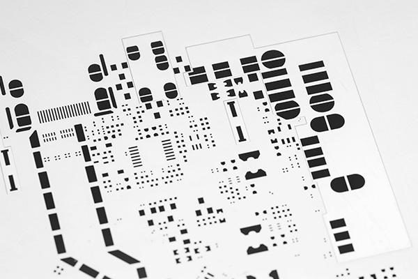
A PCB stencil is a thin, precision-cut sheet of material, typically stainless steel. It has openings, called apertures, that precisely match the solder pads on a bare PCB where surface mount components will be attached. Its purpose is to control the exact amount and location of solder paste deposited onto these pads.
Using a stencil is crucial for several reasons:
- Precision: It enables solder paste to be applied with high accuracy, even for very small and fine pitch components.
- Consistency: It ensures uniform solder paste volume across all pads, leading to consistent solder joint quality.
- Efficiency: It allows for rapid application of solder paste to an entire board or panel of boards, which is essential for mass production.
- Reliability: Proper paste deposition is the first critical step toward creating strong, defect-free solder joints that contribute to the long term reliability of electronic products.
Related Reading: The Comprehensive Guide to SMT Stencil Engineering: From Design Optimization to Process Control
Tools and Materials You Will Need
Before you begin to use a PCB stencil, gather the necessary tools and materials:
- PCB Stencil: The specific stencil designed for your PCB layout.
- Printed Circuit Boards (PCBs): The bare boards awaiting solder paste.
- Solder Paste: Ensure it is the correct type and particle size for your components and reflow profile.
- Squeegee Blade: A metal or polyurethane blade used to spread the solder paste.
- Solder Paste Printer (Automated or Manual): A machine or fixture for holding and aligning the stencil and PCB.
- Wipe Roll or Cleaning Wipes: For cleaning the stencil.
- Stencil Cleaner: Isopropyl alcohol (IPA) or a specialized stencil cleaning solution.
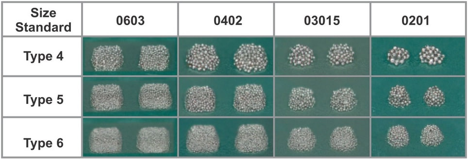
- Inspection Equipment: Magnifying lamp, microscope, or a 3D Solder Paste Inspection (SPI) system.
Step 1: Preparation is Key
Thorough preparation sets the stage for a successful solder paste printing process.
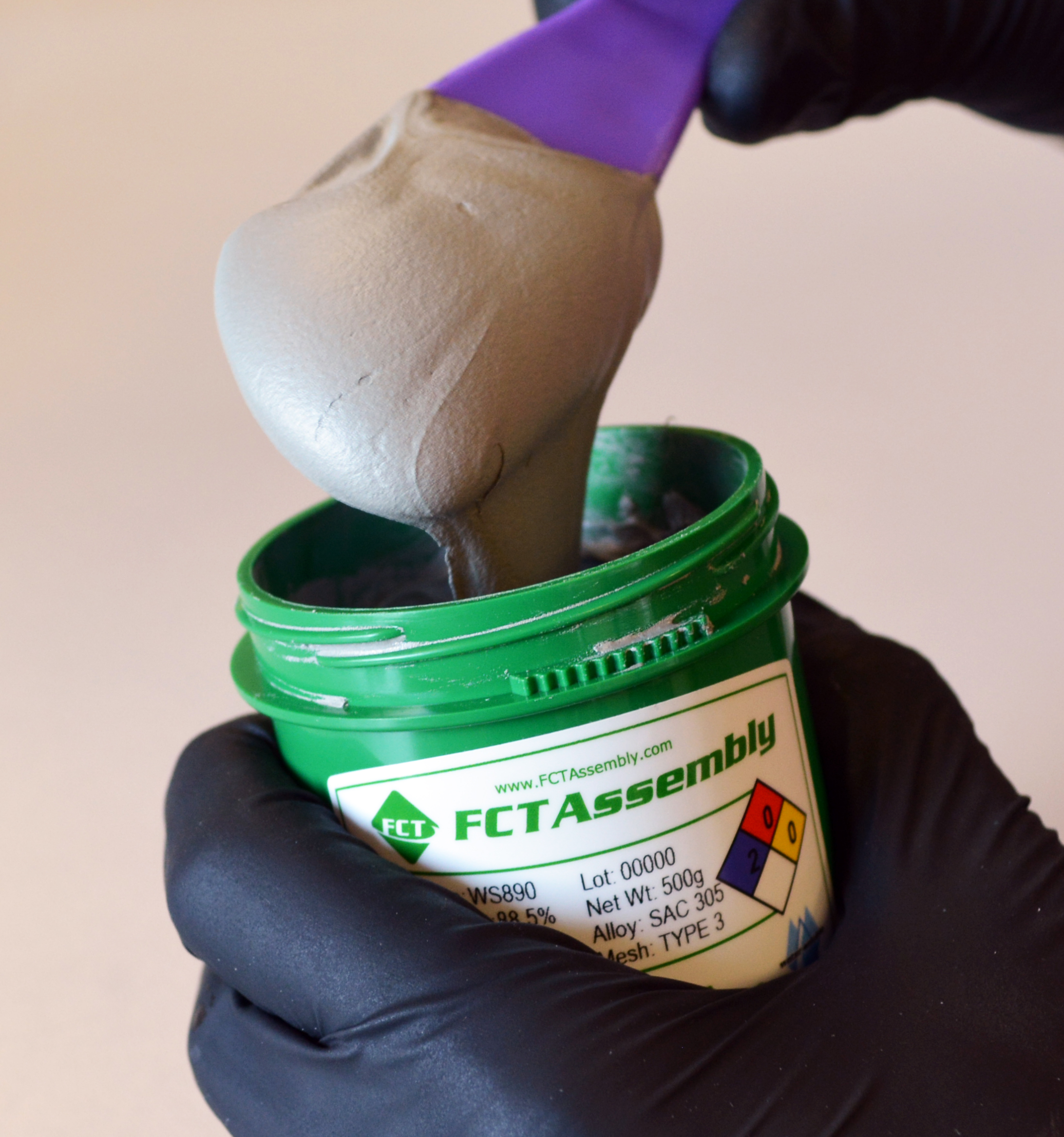
Prepare the Solder Paste
- Allow refrigerated solder paste to reach room temperature (typically 2-4 hours) before opening the jar. This prevents moisture condensation.
- Stir the solder paste thoroughly to achieve a consistent viscosity. If using a cartridge, a paste mixer can automate this.
Inspect and Clean the PCB
Ensure the PCB surface is clean and free from dust, debris, or contamination. A clean wipe with IPA can be used if necessary.
Inspect the PCB Stencil
- Check the stencil for any damage, bent edges, or clogged apertures. Use a magnifying glass or microscope to verify all apertures are clear.
- Clean the stencil if there is any residue from previous use.
Step 2: Setup and Alignment of Stencil and PCB
This step is critical for accurate solder paste deposition. The process will vary depending on whether you are using a manual or automated printer.
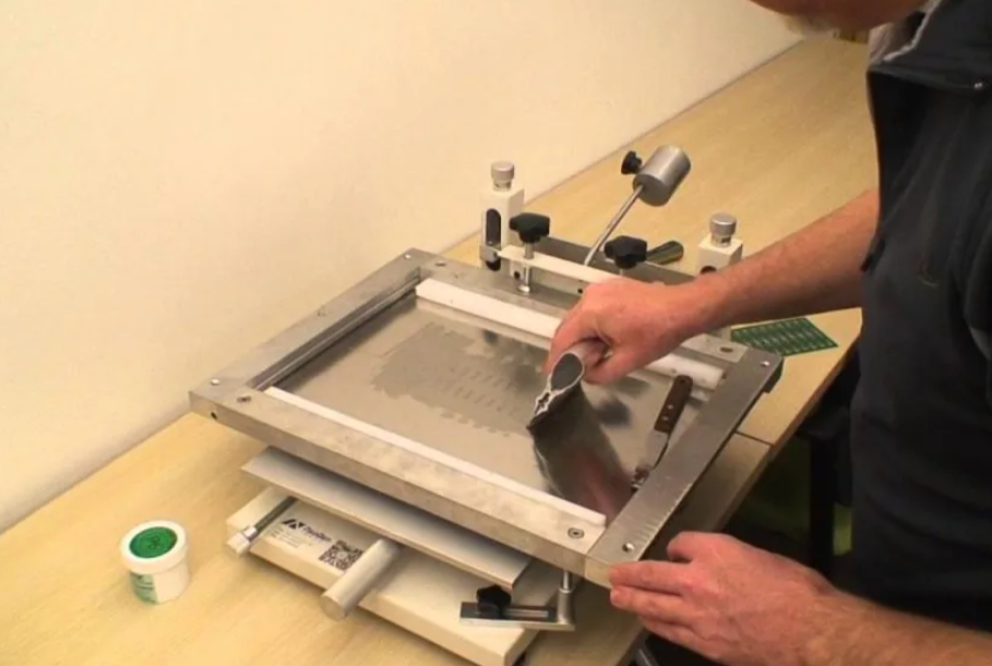
For Manual Printing (Prototype or Small Batches)
- Secure the PCB: Place your PCB onto a stable jig or fixture. Ensure it is flat and will not move during printing.
- Position the Stencil: Carefully place the stencil over the PCB.
- Align the Stencil: Align the stencil's apertures precisely with the corresponding pads on the PCB. Use visible fiducial marks on both the PCB and the stencil as alignment guides. A magnifying lamp can aid in this process. Once aligned, secure the stencil to prevent any movement.
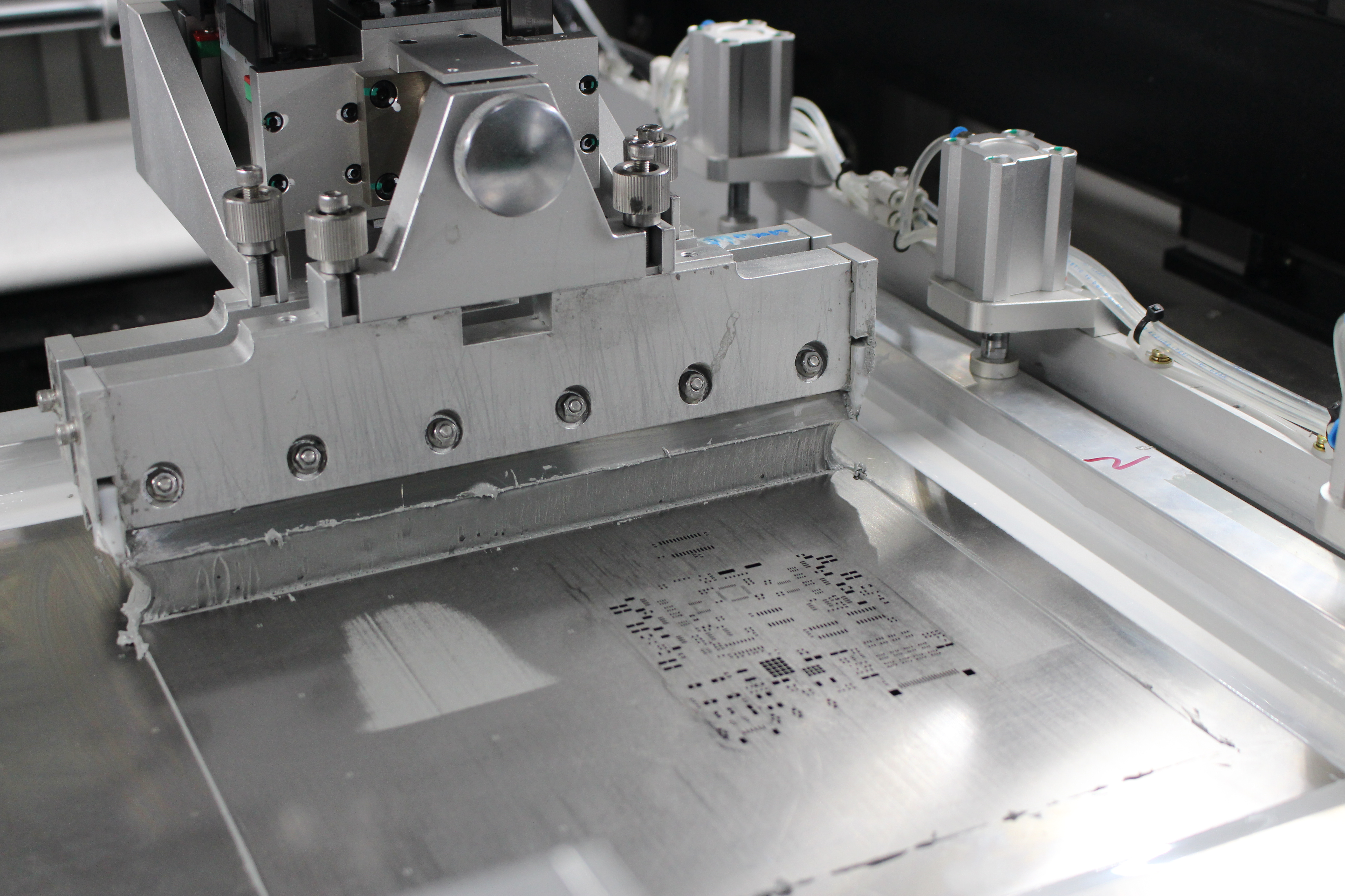
For Automated Printing (Mass Production)
- Load the PCB: The automated printer's conveyor system will transport the PCB into the print area and register it using a vision system.
- Load the Stencil: Install the framed stencil into the printer's stencil holder.
- Automated Alignment: The printer's vision system will use fiducial marks on the PCB and stencil to precisely align them. The system typically compensates for any minor translational or rotational misalignment.
Step 3: Solder Paste Application (Printing)
With the stencil and PCB aligned, it is time to apply the solder paste.
Dispense Solder Paste
Apply a "roll" of solder paste across the width of the stencil, typically in the center or slightly offset. The amount should be sufficient to cover all apertures in one or two passes.
Squeegee Stroke
- Position the Squeegee: Place the squeegee blade at one end of the solder paste roll, applying even pressure across its length.
- Apply Pressure: The pressure should be enough to ensure the squeegee makes firm contact with the stencil surface, wiping it clean as it moves. Excessive pressure can damage the stencil or scoop paste from apertures.
- Control Speed and Angle: Push or pull the squeegee across the stencil at a consistent speed and angle (typically 45-60 degrees). This forces the solder paste into the apertures, filling them completely.
- Single or Multiple Passes: Depending on the paste type and stencil design, one or two passes may be required to achieve optimal fill.
Related Reading: How Does Stencil Design Impact PCB Assembly Quality?
Stencil Separation (Snap-off)
Once the paste is applied, carefully separate the stencil from the PCB. In automated printers, this is a controlled "snap-off" process where the stencil lifts slowly and cleanly from the board. A clean separation is critical to prevent solder paste "dog ears" or smearing. The paste should remain cleanly on the PCB pads.
Step 4: Post Print Inspection (Highly Recommended)
After removing the stencil, immediate inspection of the solder paste deposits is crucial.
Visual Inspection (Manual/Automated)
Use a magnifying lamp or microscope to visually inspect the solder paste deposits on the PCB. Check for consistent paste volume, good print definition (sharp edges), absence of bridging between pads, and proper coverage on all pads.
Automated Solder Paste Inspection (SPI) (Automated Lines)
In automated lines, the PCB immediately moves to an SPI machine. This 3D inspection system automatically measures the volume, height, and area of every solder paste deposit. SPI detects defects such as insufficient paste, excessive paste, bridging, or misalignment, allowing for immediate corrective action before components are placed.
Step 5: Stencil Cleaning
Proper and timely stencil cleaning is essential to maintain print quality for subsequent boards.
Automated Underwipe (Automated Lines)
Automated printers have an integrated underwipe system. A wipe roll automatically cleans the underside of the stencil at programmable intervals (e.g., after every print or every few prints). This removes any paste residue that could cause smearing. The wipe roll may be dry, wet with solvent, or use a vacuum.
Manual Cleaning (All Processes)
- After printing a batch of boards or at the end of a shift, thoroughly clean the stencil.
- Use lint free wipes dampened with IPA or a specialized stencil cleaning solution.
- Wipe both the top and bottom surfaces of the stencil.
- Use a brush to ensure all apertures are clear of dried paste.
- Ensure the stencil is completely dry before storage.
Step 6: Reflow (The Next Step)
Once the solder paste is applied and inspected, the PCB moves to the pick and place machine for component placement, followed by the reflow oven. The reflow oven melts the solder paste, forming the electrical and mechanical connections. The quality of your solder paste print directly impacts the success of the reflow process and the final solder joint integrity.
Troubleshooting Common Stencil Issues
- Insufficient Paste: Check stencil thickness, aperture size, squeegee pressure, paste viscosity, and ensure apertures are clear.
- Excessive Paste/Bridging: Verify stencil thickness, aperture design (reduce size, windowpane), squeegee pressure, and stencil alignment.
- Smearing: Check stencil alignment, squeegee pressure, stencil cleanliness (especially underwipe), and proper separation speed.
Conclusion
Effectively using a PCB stencil is a fundamental skill in SMT assembly, directly influencing the quality and reliability of electronic products. By following this step-by-step PCB guide, from careful preparation and precise alignment to optimized solder paste application and thorough cleaning, you can ensure consistent and accurate solder paste deposition. Whether you are using a manual setup for prototyping or operating an advanced automated line, understanding these core principles of how to use a PCB stencil will empower you to minimize defects, maximize yield, and build high quality electronic assemblies.
FAQs
Q1: What is the most critical step when learning how to use a PCB stencil?
A1: The most critical step when learning how to use a PCB stencil is precise alignment of the stencil to the PCB. Any misalignment will result in solder paste misprints, leading to defects like bridging or insufficient paste on pads.
Q2: Why is it important to clean the PCB stencil regularly?
A2: It is important to clean the PCB stencil regularly because dried solder paste or residue in the apertures can block paste flow, leading to insufficient solder deposits. A clean stencil ensures consistent paste release and prevents smearing on the PCB.
Q3: Can I use a PCB stencil for both manual and automated assembly?
A3: Yes, a PCB stencil can be used for both manual and automated assembly. For manual assembly, it is typically used with a simple jig or fixture. For automated assembly, it is loaded into a specialized solder paste printer that handles alignment and squeegee operation.
Q4: What should I look for during solder paste inspection after printing?
A4: During solder paste inspection, you should look for consistent paste volume, clear print definition with sharp edges, no bridging between adjacent pads, and proper coverage on all designated pads. Automated SPI systems provide precise measurements of these parameters.
References
IPC-7525A — Stencil Design Guidelines. IPC, 2007.
J-STD-001H — Requirements for Soldered Electrical and Electronic Assemblies. IPC & JEDEC, 2020.