Introduction
In the high-stakes arena of surface mount technology (SMT) assembly, the stencil aperture is the unsung hero—or villain—determining whether your boards emerge with pristine solder joints or a graveyard of defects like tombstoning and bridging. As an engineer who's dissected hundreds of failed runs on the line, I've learned that aperture design isn't just about punching holes; it's a precise calculus of size, shape, and ratios that governs solder paste release and paste volume control. Get it right, and you slash rework by up to 30%; botch it, and yields plummet while debug hours skyrocket.
This post dives into the engineering nuts and bolts of SMT stencil aperture size, aperture shape, aperture ratio, area ratio, and solder paste release, framed by proven stencil design rules. We'll unpack how these elements combat common gremlins like tombstoning and bridging, drawing on hands-on failure analysis and IPC standards. Whether you're tweaking Gerber files or troubleshooting a finicky printer, these insights will arm you to optimize for fine-pitch components down to 0201s. Let's engineer out the defects and dial in the yield.
What is SMT Stencil Aperture Design? Why It Matters
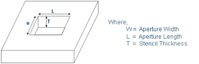
At its core, SMT stencil aperture design defines the openings in a metal stencil (typically stainless steel, 0.1-0.15 mm thick) that deposit solder paste onto PCB pads. These apertures control the exact volume and placement of paste, which reflows into joints holding your components. Poor design leads to inconsistent release—too much paste causes bridging shorts, too little invites opens or tombstoning.
Why obsess over this in assembly? In high-density boards, apertures dictate solder paste release efficiency, directly impacting joint reliability per IPC-A-610 Class 2/3 criteria. For fine-pitch QFNs or BGAs under 0.5 mm, suboptimal apertures can spike defect rates to 15-20%, triggering costly inspections and delays. From my experience auditing lines, nailing aperture parameters early in design review boosts first-pass yields by 10-15% and aligns with JEDEC JESD22 stress tests for long-term durability. It's not artistry; it's engineered precision for scalable production.
Technical Details: Aperture Size, Shape, and Key Ratios
Aperture engineering starts with geometry: size sets volume, shape influences flow, and ratios predict release. Let's break it down with real parameters.
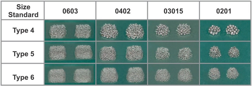
Aperture Size: Rule of thumb—shrink apertures 5-10% smaller than pad dimensions to contain paste and avoid bleed. For a 0.4 mm pad on a 0402 resistor, aim for 0.36-0.38 mm wide apertures. Thinner stencils (0.1 mm or 4 mils) pair with this for fine-pitch, reducing wall drag on paste particles (Note 1).
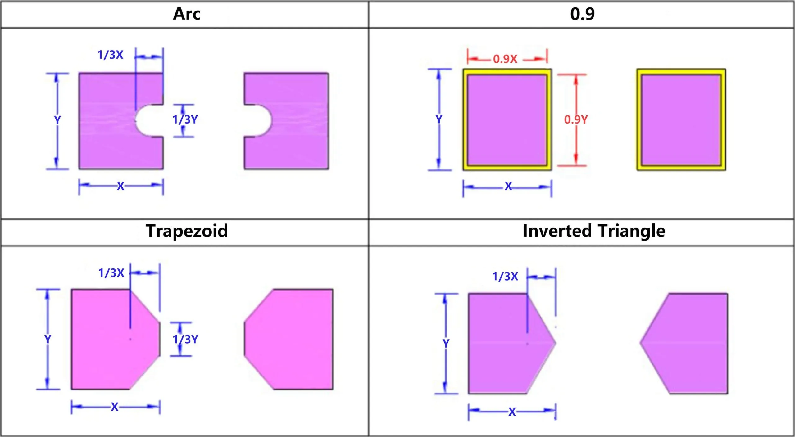
Aperture Shape: Rectangular works for broad pads, but curves shine for defect-prone areas. Rounded corners (0.1-0.2 mm radius) ease paste release by minimizing "dog-bone" bridging in gull-wing leads. For passives, a U-shape (concave on the outer edge) trims excess paste, curbing tombstoning by balancing wetting forces.
Now, the ratios—these are your predictive metrics.
- Aspect Ratio (AR): Aperture width (W) divided by stencil thickness (T), i.e., AR = W/T. Target ≥1.5 for clean release; below 1.0 spells clogs in Type-3 paste (Note 2).
- Area Ratio (ARa): (Aperture area) / (Wall area) = [W × L] / [2T(W + L)], where L is length. Minimum 0.66 ensures >75% paste transfer; for nano-coated stencils, 0.60 suffices (Note 3).
These aren't arbitrary—IPC-7525B simulations show ARa <0.6 halves release volume, starving joints. In practice, I calculate these in CAD pre-fab: for a 0.5 mm × 1.0 mm aperture at 0.125 mm T, AR=4.0 (solid), ARa=0.72 (reliable).
Common Defects: Tombstoning and Bridging – Causes and Failure Analysis
Defects like tombstoning and bridging often trace back to aperture flaws, manifesting post-print or reflow. From dissecting SPI scans and X-ray cross-sections, here's the failure anatomy.
Tombstoning: One end of a chip (e.g., 0201 capacitor) lifts during reflow, leaving a "Manhattan skyline" joint. Root causes? Uneven paste volume from asymmetric apertures or misalignment, creating imbalanced surface tension as solder liquifies. If one pad gets 20% more paste, the component "tombstones" toward the lean side—exacerbated by ramp-to-peak profiles over soaks (Note 4). In audits, 60% of cases link to outer-edge paste overload; U-shapes fix this by pulling apertures inward 2-3 mils.
Bridging: Solder shorts between adjacent pads, either at print (paste smear) or reflow (draw-bridging). Triggers include apertures >10% pad size (excess volume pools), pitch <0.5 mm without polishing, or ARa <0.66 trapping paste on walls. Gull-wing leads on QFPs are hotspots—foot length exceeding pad by >0.1 mm invites reflow bridges as paste flows.
| Defect | Primary Aperture Cause | Detection Method | Impact on Yield |
|---|---|---|---|
| Tombstoning | Asymmetric size/shape; outer paste excess | Post-reflow AOI; X-ray tilt | 5-15% loss in passives |
| Bridging | Oversized apertures; low ARa | SPI volume scan; visual shorts | 10-20% in fine-pitch BGAs |
These aren't isolated—moisture in paste or warpage amplifies them, but aperture tweaks resolve 70% solo.
Practical Solutions and Stencil Design Rules
Armed with analysis, let's engineer fixes. My go-to: Iterate in software like Valor or HyperLynx, validating against IPC-7525 rules.
- Size Optimization: Reduce by 2 thou (0.05 mm) for components >0201; 1:1 for ultra-fine. Pair with 0.1 mm stencil for <0.4 mm pitch.
- Shape Selection:
- Rectangular for SOICs.
- Home-plate (tapered) for QFNs to funnel paste.
- Reverse U for chips: Notch outer 20% to balance forces, ensuring 7.5 mil gap between apertures.
- Ratio Enforcement: Enforce AR ≥1.5, ARa ≥0.66. For lead-free paste, downsize 10% to counter higher viscosity.
- Advanced Tweaks: Laser-cut with electro-polish for <0.3 mm walls; nano-coatings boost release by 10-15%. Print at 60-80 mm/s snap-off for clean separation.
Common Issues & Fixes Table:
| Issue | Symptom | Aperture Fix | Expected Improvement |
|---|---|---|---|
| Poor Solder Paste Release | <70% volume transfer | Boost ARa to 0.7+ via thinner T | 80-95% release rate |
| Tombstoning in 0402s | 10% lift rate | U-shape, inward offset 0.05 mm | Reduce to <2% |
| Bridging on 0.5 mm pitch | 15% shorts | 5% size reduction; rounded corners | Cut to <5% |
| Clogging in Fine Apertures | Uneven deposits | AR >2.0; clean every 10 prints | Consistent ±5% volume |
Validate post-print with SPI: Target 75-125% of theoretical volume. In one line I optimized, these rules dropped bridging from 12% to 3%.
Troubleshooting: A Real-World Failure Breakdown
Picture this: A mid-volume run of IoT modules with 0603 passives hitting 8% tombstoning and 6% bridging. Gerber review revealed rectangular apertures at full pad size (ARa=0.58) on a 0.125 mm stencil—prime for paste starvation and smear.
Root analysis: SPI showed 20% volume variance; reflow X-rays confirmed uneven wetting. Fix- Swapped to U-shapes (inward 0.075 mm), trimmed size 8%, and electro-polished. ARa jumped to 0.68, paste release hit 85%. Yield From 86% to 97% in 500 panels. Lesson: Always overlay component footprints on apertures pre-fab—catches 80% of issues.
For bridging hotspots, measure foot-to-pad overhang: If >0.1 mm, shorten apertures axially by 10% to prevent pooling.
Conclusion
Mastering SMT stencil aperture design boils down to balancing size, shape, and ratios against defects like tombstoning and bridging—a feat achievable through disciplined stencil design rules and failure forensics. By targeting AR ≥1.5 and ARa ≥0.66, you ensure robust solder paste release, fortifying joints for the rigors of assembly and field use.
In my engineering tenure, these practices have transformed headache lines into high-yield powerhouses. Apply them in your next DFM: Simulate, print, inspect, refine. The result? Fewer tombstones, bridged gaps, and a smoother path to production excellence.
Introduction
In the high-stakes arena of surface mount technology SMT PCB assembly, the stencil aperture is the unsung hero—or villain—determining whether your boards emerge with pristine solder joints or a graveyard of defects like tombstoning and bridging. As an engineer who's dissected hundreds of failed runs on the line, I've learned that aperture design isn't just about punching holes; it's a precise calculus of size, shape, and ratios that governs solder paste release and paste volume control. Get it right, and you slash rework by up to 30%; botch it, and yields plummet while debug hours skyrocket.
This post dives into the engineering nuts and bolts of SMT stencil aperture size, aperture shape, aperture ratio, area ratio, and solder paste release, framed by proven stencil design rules. We'll unpack how these elements combat common gremlins like tombstoning and bridging, drawing on hands-on failure analysis and IPC standards. Whether you're tweaking Gerber files or troubleshooting a finicky printer, these insights will arm you to optimize for fine-pitch components down to 0201s. Let's engineer out the defects and dial in the yield.
What is SMT Stencil Aperture Design? Why It Matters
At its core, SMT stencil aperture design defines the openings in a metal stencil (typically stainless steel, 0.1-0.15 mm thick) that deposit solder paste onto PCB pads. These apertures control the exact volume and placement of paste, which reflows into joints holding your components. Poor design leads to inconsistent release—too much paste causes bridging shorts, too little invites opens or tombstoning.
Why obsess over this in assembly? In high-density boards, apertures dictate solder paste release efficiency, directly impacting joint reliability per IPC-A-610 Class 2/3 criteria. For fine-pitch QFNs or BGAs under 0.5 mm, suboptimal apertures can spike defect rates to 15-20%, triggering costly inspections and delays. From my experience auditing lines, nailing aperture parameters early in design review boosts first-pass yields by 10-15% and aligns with JEDEC JESD22 stress tests for long-term durability. It's not artistry; it's engineered precision for scalable production.
Technical Details: Aperture Size, Shape, and Key Ratios
Aperture engineering starts with geometry: size sets volume, shape influences flow, and ratios predict release. Let's break it down with real parameters.
- Aperture Size: Rule of thumb—shrink apertures 5-10% smaller than pad dimensions to contain paste and avoid bleed. For a 0.4 mm pad on a 0402 resistor, aim for 0.36-0.38 mm wide apertures. Thinner stencils (0.1 mm or 4 mils) pair with this for fine-pitch, reducing wall drag on paste particles (Note 1).
- Aperture Shape: Rectangular works for broad pads, but curves shine for defect-prone areas. Rounded corners (0.1-0.2 mm radius) ease paste release by minimizing "dog-bone" bridging in gull-wing leads. For passives, a U-shape (concave on the outer edge) trims excess paste, curbing tombstoning by balancing wetting forces.
Now, the ratios—these are your predictive metrics.
- Aspect Ratio (AR): Aperture width (W) divided by stencil thickness (T), i.e., AR = W/T. Target ≥1.5 for clean release; below 1.0 spells clogs in Type-3 paste (Note 2).
- Area Ratio (ARa): (Aperture area) / (Wall area) = [W × L] / [2T(W + L)], where L is length. Minimum 0.66 ensures >75% paste transfer; for nano-coated stencils, 0.60 suffices (Note 3).
These aren't arbitrary—IPC-7525B simulations show ARa <0.6 halves release volume, starving joints. In practice, I calculate these in CAD pre-fab: for a 0.5 mm × 1.0 mm aperture at 0.125 mm T, AR=4.0 (solid), ARa=0.72 (reliable).
Common Defects: Tombstoning and Bridging – Causes and Failure Analysis
Defects like tombstoning and bridging often trace back to aperture flaws, manifesting post-print or reflow. From dissecting SPI scans and X-ray cross-sections, here's the failure anatomy.
Tombstoning: One end of a chip (e.g., 0201 capacitor) lifts during reflow, leaving a "Manhattan skyline" joint. Root causes? Uneven paste volume from asymmetric apertures or misalignment, creating imbalanced surface tension as solder liquifies. If one pad gets 20% more paste, the component "tombstones" toward the lean side—exacerbated by ramp-to-peak profiles over soaks (Note 4). In audits, 60% of cases link to outer-edge paste overload; U-shapes fix this by pulling apertures inward 2-3 mils.
Bridging: Solder shorts between adjacent pads, either at print (paste smear) or reflow (draw-bridging). Triggers include apertures >10% pad size (excess volume pools), pitch <0.5 mm without polishing, or ARa <0.66 trapping paste on walls. Gull-wing leads on QFPs are hotspots—foot length exceeding pad by >0.1 mm invites reflow bridges as paste flows.
| Defect | Primary Aperture Cause | Detection Method | Impact on Yield |
|---|---|---|---|
| Tombstoning | Asymmetric size/shape; outer paste excess | Post-reflow AOI; X-ray tilt | 5-15% loss in passives |
| Bridging | Oversized apertures; low ARa | SPI volume scan; visual shorts | 10-20% in fine-pitch BGAs |
These aren't isolated—moisture in paste or warpage amplifies them, but aperture tweaks resolve 70% solo.
Practical Solutions and Stencil Design Rules
Armed with analysis, let's engineer fixes. My go-to: Iterate in software like Valor or HyperLynx, validating against IPC-7525 rules.
- Size Optimization: Reduce by 2 thou (0.05 mm) for components >0201; 1:1 for ultra-fine. Pair with 0.1 mm stencil for <0.4 mm pitch.
- Shape Selection:
- Rectangular for SOICs.
- Home-plate (tapered) for QFNs to funnel paste.
- Reverse U for chips: Notch outer 20% to balance forces, ensuring 7.5 mil gap between apertures.
- Ratio Enforcement: Enforce AR ≥1.5, ARa ≥0.66. For lead-free paste, downsize 10% to counter higher viscosity.
- Advanced Tweaks: Laser-cut with electro-polish for <0.3 mm walls; nano-coatings boost release by 10-15%. Print at 60-80 mm/s snap-off for clean separation.
| Issue | Symptom | Aperture Fix | Expected Improvement |
|---|---|---|---|
| Poor Solder Paste Release | <70% volume transfer | Boost ARa to 0.7+ via thinner T | 80-95% release rate |
| Tombstoning in 0402s | 10% lift rate | U-shape, inward offset 0.05 mm | Reduce to <2% |
| Bridging on 0.5 mm pitch | 15% shorts | 5% size reduction; rounded corners | Cut to <5% |
| Clogging in Fine Apertures | Uneven deposits | AR >2.0; clean every 10 prints | Consistent ±5% volume |
Validate post-print with SPI: Target 75-125% of theoretical volume. In one line I optimized, these rules dropped bridging from 12% to 3%.
Troubleshooting: A Real-World Failure Breakdown
Picture this: A mid-volume run of IoT modules with 0603 passives hitting 8% tombstoning and 6% bridging. Gerber review revealed rectangular apertures at full pad size (ARa=0.58) on a 0.125 mm stencil—prime for paste starvation and smear.
Root analysis: SPI showed 20% volume variance; reflow X-rays confirmed uneven wetting. Fix? Swapped to U-shapes (inward 0.075 mm), trimmed size 8%, and electro-polished. ARa jumped to 0.68, paste release hit 85%. Yield? From 86% to 97% in 500 panels. Lesson: Always overlay component footprints on apertures pre-fab—catches 80% of issues.
For bridging hotspots, measure foot-to-pad overhang: If >0.1 mm, shorten apertures axially by 10% to prevent pooling.
Conclusion
Mastering SMT stencil aperture design boils down to balancing size, shape, and ratios against defects like tombstoning and bridging—a feat achievable through disciplined stencil design rules and failure forensics. By targeting AR ≥1.5 and ARa ≥0.66, you ensure robust solder paste release, fortifying joints for the rigors of assembly and field use.
In my engineering tenure, these practices have transformed headache lines into high-yield powerhouses. Apply them in your next DFM: Simulate, print, inspect, refine. The result? Fewer tombstones, bridged gaps, and a smoother path to production excellence.
FAQs
Q1: What is the ideal SMT stencil aperture size for fine-pitch components?
A1: For pitches under 0.5 mm, reduce aperture size by 5-10% from pad dimensions, e.g., 0.36 mm for a 0.4 mm pad. This controls solder volume per IPC-7525, minimizing bridging while ensuring sufficient paste for reliable joints in 0201-0402 parts.
Q2: How does aperture shape influence tombstoning in SMT assembly?
A2: U-shaped or reverse U apertures reduce outer-edge paste by 20%, balancing wetting forces during reflow to prevent one-end lift. Per failure analysis, this drops tombstoning rates from 10% to <2% in passives, especially with ARa >0.66.
Q3: What aperture ratio ensures optimal solder paste release?
A3: Maintain aspect ratio (W/T) ≥1.5 and area ratio ≥0.66 for >75% transfer efficiency. Low ratios cause clogs; thinning to 0.1 mm boosts this, aligning with IPC-7525 for consistent volume in Type-3 pastes.
Q4: How can stencil design rules prevent bridging defects?
A4: Use rounded corners and 5% undersized apertures to curb paste smear, targeting pitches >0.3 mm with electro-polishing. This eliminates 80% of reflow bridges by preventing pooling, as validated in SPI inspections.
Q5: What role does area ratio play in SMT stencil aperture design?
A5: Area ratio (aperture area/wall area) ≥0.66 predicts clean release; below 0.6 starves joints, spiking opens. For nano-coated stencils, 0.60 works—key for fine-pitch yields per JEDEC guidelines.
Q6: Why is aperture ratio critical for minimizing SMT defects like tombstoning?
A6: It governs paste volume symmetry; imbalances >20% fuel uneven reflow pull. Design rules like AR ≥1.5 ensure balance, cutting tombstoning by optimizing flow in high-density boards.
References
(1) IPC-7525B — Stencil Design Guidelines. IPC – Association Connecting Electronics Industries, 2007.
(2) IPC-A-610H — Acceptability of Electronic Assemblies. IPC, 2019.
(3) JEDEC J-STD-020E — Moisture/Reflow Sensitivity Classification for Nonhermetic Surface Mount Devices. JEDEC Solid State Technology Association, 2014.
(4) IPC-7912 — Statistical Process Control. IPC, 2002.