Introduction
Correct SMT stencil pad design is the foundation of reliable, high-yield surface-mount assembly. Even perfect PCB layout and premium solder paste will fail if the stencil apertures do not deliver the right volume and shape of paste to every pad. Beginners often copy PCB pad size 1:1 into the stencil, resulting in excessive solder, tombstoning, bridging, or insufficient heel fillets. This practical guide explains step-by-step rules, aperture shapes, reduction formulas, and real-world adjustments that assembly engineers apply every day to achieve defect-free soldering from 01005 chips to large QFN thermal pads.
Why Stencil Apertures Are Never 1:1 with PCB Pads
Solder paste is roughly 50% metal and 50% flux by volume. After reflow, paste volume reduces dramatically. The SMD stencil must therefore release more paste than the final solder joint requires. Aperture size, shape, and wall smoothness directly control paste transfer efficiency. Industry data shows transfer efficiency ranges from 60% on fine-pitch to nearly 100% on large pads. Beginners who use 1:1 apertures usually experience:
- Bridging on 0.4–0.5 mm pitch QFP and chips
- Tombstoning on 0201 and 01005 resistors
- Insufficient heel fillets on SOIC and QFN
- Voiding on large thermal pads
Basic Aperture Modification Rules (IPC-7525A Guidelines)
Standard Rectangular Chip Components (0402 and larger)
- Length reduction: 0% (keep same as pad length)
- Width reduction: 10% (or 0.1–0.15 mm total)
- Corner radius: 0.1–0.2 mm (home-plate shape optional for 0603 and larger)
Small Chip Components (0201 and 01005)
- Use square-end apertures
- Reduce width by 15–20%
- Never round corners (reduces volume too much)
SOT, SOD, QFP, and Gull-Wing Leads
- Home-plate (inverted trapezoid) shape is standard
- Reduce pad width by 10–15% at toe and heel
- Keep aperture length 0.9–1.0× pad length
- Rounded corners 0.075–0.15 mm radius
BGA and LGA Pads (non-solder-mask-defined)
- Circular apertures
- Diameter = 0.9–1.0× pad diameter (most common 1:1)
- 0.5 mm pitch and finer: stay 1:1
- 0.8 mm pitch and coarser: 0.95× or 1:1
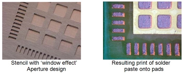
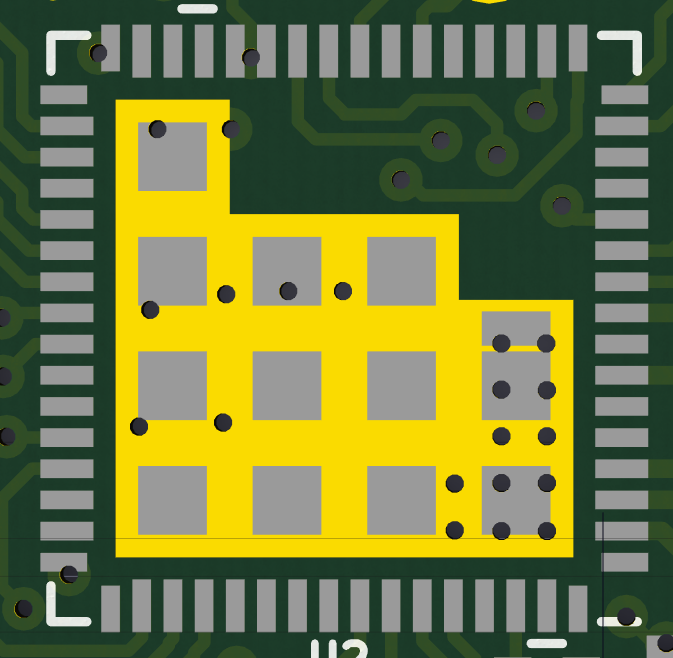
QFN and Large Thermal Pads
- Never use one large square aperture
- Use window-pane (grid) or segmented pattern
- Total open area 50–70% of pad area
- Individual segment width 0.5–1.0 mm
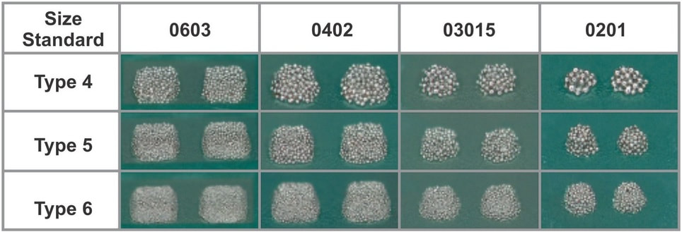
Stencil Thickness Selection Table
| Component Type | Pitch | Recommended Thickness | Typical Paste Type |
|---|---|---|---|
| 01005, 0201, 0.4 mm BGA | ≤0.4 mm | 80–100 µm | Type 5 or 6 |
| 0402, 0.5 mm BGA | 0.5 mm | 100–120 µm | Type 4 or 5 |
| 0603–1206, 0.8–1.0 mm | ≥0.65 mm | 125–150 µm | Type 3 or 4 |
| QFN, connectors | Large pads | 150–200 µm | Type 3 |
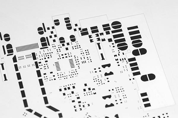
Step-by-Step Stencil Design Process for Beginners
- Start with Gerber data of solder-mask layer (not copper layer)
- Apply global 10% width reduction to all rectangular chip pads
- Change QFP/SOIC apertures to home-plate shape with 0.1 mm corner radius
- Keep BGA apertures circular 1:1
- Segment all thermal pads >4×4 mm into 0.8 mm wide strips or 1 mm squares
- Add two half-etched fiducial marks on opposite corners
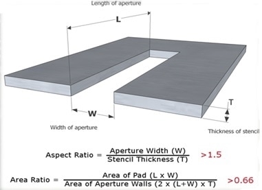
- Verify aperture area ratio >0.66 and aspect ratio >1.5 for every opening
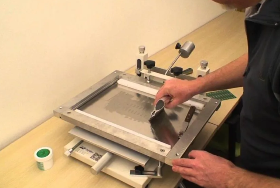
- Export final Gerber and send for laser-cut, electro-polished stencil
Area Ratio and Aspect Ratio Explained
- Aspect ratio = aperture width / stencil thickness Must be ≥1.5 for good paste release
- Area ratio = aperture area / wall area = (L × W) / (2 × T × (L + W)) Must be ≥0.66 for reliable transfer (0.60 minimum for Type 5 paste)
Example: 0.25 mm wide aperture in 100 µm foil Aspect ratio = 0.25 / 0.1 = 2.5 → good Area ratio ≈ 0.625 → marginal, consider 80 µm foil instead
Common Beginner Mistakes and Fixes
| Mistake | Result | Fix |
|---|---|---|
| 1:1 apertures on chip components | Tombstoning, bridging | Reduce width 10–15% |
| Rounded corners on 0201 | Insufficient volume | Use square corners |
| Single large aperture on QFN pad | Large voids | Segment into window-pane |
| Stencil thickness too thin for QFN | Poor heel fillet | Increase to 150–180 µm |
| No fiducials on stencil | Misalignment | Add two global fiducials |
Conclusion
Mastering SMT stencil pad design is the fastest way for beginners to improve assembly yield. In fact, these same stencil design rules are standard practice at any large PCB manufacturer, where consistent paste release is critical for high-volume production. Start with the standard 10% width reduction for chip components, home-plate shapes for gull-wing leads, 1:1 circles for BGA, and window-pane patterns for thermal pads. Always verify an area ratio of ≥ 0.66 and select stencil thickness according to the finest pitch on the board. Following these practical, field-proven guidelines helps eliminate most soldering defects before the first board even reaches the printer.
FAQs
Q1: Should I always use 1:1 apertures for BGA pads in SMT stencil pad design?
A1: Yes. BGA pads are non-solder-mask-defined and self-centering. 1:1 circular apertures with electro-polished walls give optimal transfer efficiency and minimal voiding.
Q2: Why do we reduce aperture width on chip components but not length?
A2: Width reduction prevents excess paste from squeezing out sideways during reflow. Length is kept full to ensure strong heel and toe fillets.
Q3: Can I use the same stencil thickness for 0201 and large connectors?
A3: No. Fine-pitch requires 80–100 µm foil, while connectors and QFN need 150–200 µm. Multi-level (step) stencils are common in mixed-technology boards.
Q4: What is the simplest way to segment a QFN thermal pad?
A4: Create a grid of 0.8–1.0 mm wide strips or squares with 0.2–0.3 mm walls between them. Total open area should be 50–65%.
References
IPC-7525B — Stencil Design Guidelines. IPC, 2011.
IPC-7095D — Design and Assembly Process Implementation for BGAs. IPC, 2018.
IPC-7527 — Requirements for Solder Paste Printing. IPC, 2012.
IPC-TM-650 2.4.28 — Solder Paste Viscosity Measurement. IPC, 2018.