Introduction
In the intricate world of electronics manufacturing, the surface mount technology (SMT) stencil stands as a cornerstone of the PCB assembly process. It is a precision tool that dictates the precise volume and placement of solder paste, which forms the critical electrical and mechanical connections between components and the printed circuit board. As an assembly engineer, I have witnessed firsthand how a well-designed and properly utilized SMT stencil is fundamental to achieving high yield, superior quality, and reliable electronic products. Conversely, errors in SMT stencil design guide principles or improper handling can lead to costly defects and rework. This comprehensive guide will navigate the journey of SMT stencils, from initial design considerations and material selection to practical solder paste application techniques and common troubleshooting scenarios.
What is an SMT Stencil and Its Role in PCB Assembly
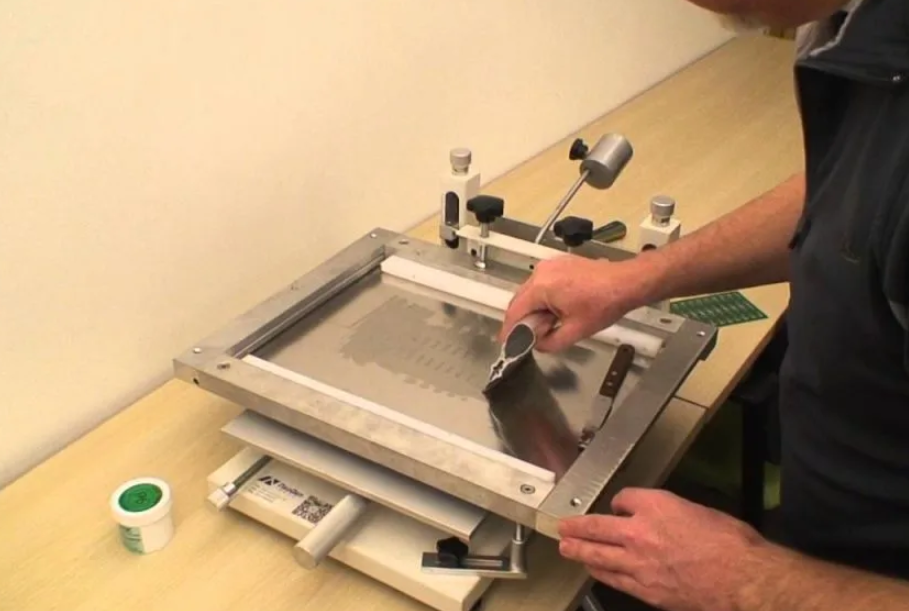
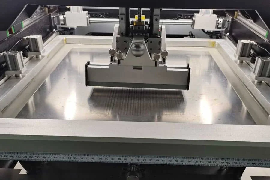
An SMT stencil is a thin sheet, typically made of stainless steel, nickel, or a nickel alloy, with a pattern of openings (apertures) corresponding to the solder pads on a PCB. During the PCB assembly process, the stencil is placed in intimate contact with the PCB. Solder paste is then applied to the stencil's top surface using a squeegee blade. The squeegee forces the solder paste through the apertures, depositing a controlled amount onto each designated pad on the PCB.
The stencil's role is absolutely critical for several reasons:
- Precision and Repeatability: It ensures that solder paste is deposited accurately and consistently on every pad, which is vital for fine pitch components.
- Volume Control: The stencil's thickness and aperture dimensions precisely control the volume of solder paste, optimizing solder joint formation.
- Efficiency: It enables the rapid and simultaneous application of solder paste to hundreds or thousands of pads, facilitating high speed automated assembly.
- Quality and Reliability: Proper paste deposition directly impacts the quality, strength, and electrical integrity of the final solder joints, contributing to overall product reliability.
Related Reading: The Comprehensive Guide to SMT Stencil Engineering: From Design Optimization to Process Control
Key Design Considerations for SMT Stencils
Effective stencil design is a crucial step that directly impacts the success of the entire PCB assembly process. Adherence to an SMT stencil design guide is essential.
1. Stencil Thickness
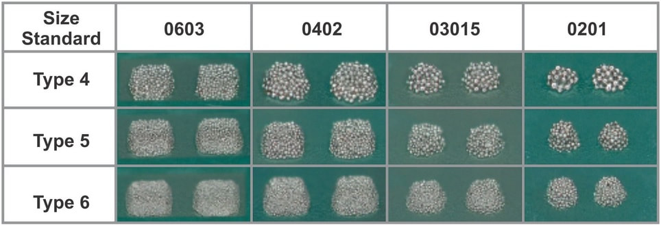
The stencil's thickness is a primary factor determining the volume of solder paste deposited. The selection of stencil thickness is a delicate balance. A thinner stencil reduces paste volume, preventing bridging on fine pitch components (e.g., 0.4 mm pitch ICs, 01005 passives). However, it may provide insufficient paste for larger components (e.g., 1210 capacitors, thermal pads of QFNs) leading to opens or weak joints. Conversely, a thicker stencil ensures robust joints for larger components but increases the risk of bridging on fine pitch pads. IPC-7525A, Stencil Design Guidelines, provides recommendations for stencil thickness selection based on component pitch.
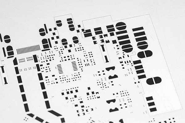
2. Aperture Design Rules
The design of each individual aperture is paramount for consistent paste release and optimal solder joint formation. These aperture design rules are critical.
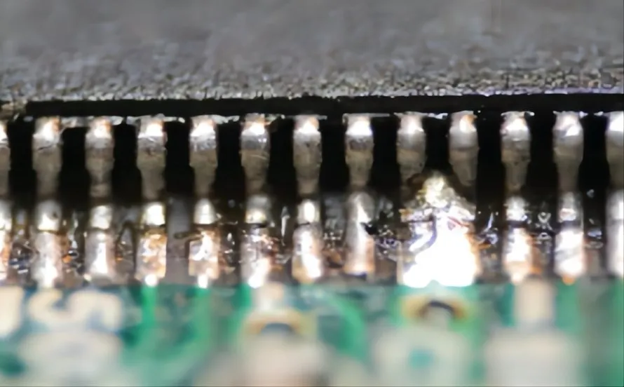
- Aperture Reduction: For fine pitch components (e.g., 0.5 mm pitch and smaller), apertures are often reduced (e.g., by 10-20% in area) compared to the actual pad size. This compensates for slight stencil movement and minimizes bridging.
- Windowpaning/Multiple Openings: For large thermal pads (e.g., under QFNs, BGAs), a single large aperture can cause excessive solder paste and voiding. Breaking this into multiple smaller openings or a grid pattern (windowpaning) helps control paste volume, promotes outgassing during reflow, and reduces voids, improving thermal performance and reliability.
- Home Plate/U-Shape: For specific component leads (e.g., gull wing leads), modifying the aperture shape (e.g., a "home plate" or U-shape) can optimize paste brick formation and minimize solder balls.
- Aspect Ratio and Area Ratio: As mentioned in previous discussions, for consistent paste release, the aspect ratio (aperture width to stencil thickness) should ideally be greater than 1.5. The area ratio (aperture area to aperture wall area) should be greater than 0.66. These ratios are fundamental aperture design rules to prevent paste from sticking to stencil walls.
3. Fiducial Marks
Fiducial marks are optically recognized targets on both the PCB and the stencil. They enable precise alignment of the stencil to the PCB using a vision system during the solder paste printing process. Both global fiducials (for overall board alignment) and local fiducials (for fine pitch component alignment) are critical.
4. Frame and Mounting
Stencils are typically mounted in frames to provide tension and stability. Framed stencils are commonly used in automated solder paste printers. Frame dimensions and mounting methods must be compatible with the printing equipment.
Related Reading: How Does Stencil Design Impact PCB Assembly Quality?
Stencil Material Selection
The choice of stencil material selection impacts stencil durability, precision, and paste release characteristics.
1. Stainless Steel Stencils
- Advantages: Most common and cost-effective. Good mechanical strength and durability. Suitable for a wide range of applications.
- Disadvantages: Can be challenging to create very fine features for ultra fine pitch components using traditional etching. Laser cutting offers better precision.
2. Nickel Stencils
- Advantages: Better fatigue resistance and smoother aperture walls than stainless steel. Offers improved paste release, especially for fine pitch components.
- Disadvantages: Slightly higher cost than stainless steel.
3. Electroformed Stencils
- Advantages: Created through an additive electrochemical process, resulting in extremely smooth trapezoidal aperture walls and very precise, fine features. Offers superior paste release, excellent for ultra fine pitch components (e.g., 0.3 mm pitch), and reduced bridging.
- Disadvantages: Highest cost among stencil types. Can be more fragile than stainless steel.
Solder Paste Application Techniques
Beyond stencil design, proper solder paste application techniques are vital for successful PCB assembly process.
1. Printer Setup Parameters
- Squeegee Type: Metal squeegee blades are typically preferred over polyurethane for fine pitch printing due to their rigidity and ability to create a clean wipe.
- Squeegee Pressure: Optimized pressure ensures good stencil-to-board contact without damaging the stencil or the board. Excessive pressure can lead to paste smearing or scooping.
- Squeegee Speed: The speed at which the squeegee travels across the stencil influences paste rolling and aperture filling. Too fast or too slow can lead to insufficient paste or smearing.
- Separation Speed (Snap-off Speed): The speed at which the stencil separates from the PCB after printing. A slow, controlled separation minimizes paste sticking to the stencil walls, improving paste release and reducing defects like "dog ears."
- Print Gap (Underwipe Gap): The distance between the bottom of the stencil and the top of the PCB. Modern printers use an "on-contact" printing method with zero print gap.
2. Solder Paste Inspection (SPI)
Three-dimensional SPI systems are indispensable in modern SMT lines. They perform automated inspection of every solder paste deposit immediately after printing. SPI verifies paste volume, height, area, and shape. This early detection of printing defects is crucial for preventing costly rework after reflow and maintaining high yield in the PCB assembly process.
3. Stencil Cleaning
Regular and thorough stencil cleaning is fundamental.
- Automated Underwipe: Most SMT printers include an automated underwipe system that cleans the bottom of the stencil at set intervals using a wipe roll (dry, wet, or vacuum).
- Manual Cleaning: Operators perform manual cleaning of the stencil top surface and apertures to remove dried paste or debris. Clean apertures are essential for consistent paste release.
Common Stencil-Related Defects and Troubleshooting
From experience, many assembly defects can be traced back to the stencil or the printing process.
- Insufficient Solder Paste:
- Symptoms: Opens, weak solder joints, insufficient fillets, component tombstoning (for smaller components).
- Causes: Stencil too thin for desired paste volume, apertures too small, poor aspect/area ratio causing paste to stick in apertures, clogged apertures, insufficient squeegee pressure, or improper paste rheology.
- Troubleshooting: Adjust aperture design, use a thicker stencil or step-up stencil, optimize printing parameters (squeegee pressure, speed, separation), ensure proper stencil cleaning.
- Excessive Solder Paste:
- Symptoms: Bridging (solder shorts between pads), solder balls, excessive fillets, head-in-pillow defect (for BGAs/QFNs).
- Causes: Stencil too thick, apertures too large, poor aperture design for specific component, stencil misalignment, excessive squeegee pressure, or improper paste rheology.
- Troubleshooting: Reduce aperture size or use step-down stencil, ensure precise stencil alignment, optimize printing parameters.
- Solder Paste Smearing:
- Symptoms: Solder paste trails or residue on the board between pads.
- Causes: Stencil-to-board misalignment, excessive squeegee pressure, worn squeegee blade, insufficient stencil cleaning (especially underwipe), or paste sticking to the bottom of the stencil.
- Troubleshooting: Verify alignment, adjust pressure, replace squeegee, improve cleaning cycles.
- Head-in-Pillow (HIP):
- Symptoms: Non-wetting defect where the component solder ball sits on top of the reflowed solder paste, resembling a "head in a pillow," indicating a poor connection.
- Causes: Often a complex issue, but stencil-related causes include insufficient paste volume on BGA pads, poor paste print definition, or excessive oxidation of component solder balls.
- Troubleshooting: Optimize paste volume, improve paste release from apertures, ensure fresh paste, and inspect component quality.
Conclusion
The SMT stencil is far more than just a metal sheet with holes; it is a precision tool critical to the success of the entire PCB assembly process. From adhering to robust SMT stencil design guide principles, including meticulous aperture design rules and appropriate stencil material selection, to implementing meticulous solder paste application techniques, every stage impacts the quality of the final product. By understanding and diligently controlling these variables, assembly engineers can effectively manage the delicate balance of solder paste deposition for a diverse range of components, minimizing defects and maximizing yield. This comprehensive approach ensures that every component stencil detailed guide contributes to reliable and high performance electronic assemblies.
FAQs
Q1: What are the main factors in selecting the correct SMT stencil thickness?
A1: The main factors in selecting the correct SMT stencil thickness are the pitch of the smallest components, the overall component mix (fine pitch vs. large), solder paste particle size, and desired solder paste volume. IPC-7525A provides guidelines.
Q2: How do aperture design rules prevent solder paste defects?
A2: Aperture design rules prevent solder paste defects by optimizing the size and shape of stencil openings. Techniques like aperture reduction, windowpaning, and ensuring good aspect/area ratios minimize bridging for fine pitch parts and reduce voids for larger thermal pads.
Q3: What is the advantage of using an electroformed stencil over a stainless steel stencil?
A3: The main advantage of an electroformed SMT stencil over a stainless steel stencil is its superior precision and smoother trapezoidal aperture walls. This provides significantly better solder paste release, making it ideal for ultra fine pitch components and reducing defects like bridging.
Q4: Why is Solder Paste Inspection (SPI) important in the PCB assembly process?
A4: SPI is important in the PCB assembly process because it performs automated 3D inspection of every solder paste deposit immediately after printing. This allows for early detection of printing defects in paste volume, height, and shape, preventing costly rework after reflow.
References
IPC-7525A — Stencil Design Guidelines. IPC, 2007.
IPC-7525C — Stencil Design Guidelines. IPC, 2022.
J-STD-001H — Requirements for Soldered Electrical and Electronic Assemblies. IPC & JEDEC, 2020.