










Microvia Voiding
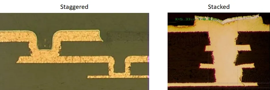
Microvia voiding is a critical defect in printed circuit board (PCB) manufacturing, where voids or gaps form within the plated or filled microvias, potentially compromising electrical connectivity and long-term reliability. These tiny vias, often less than 150 microns in diameter, are essential for high-density interconnects in modern electronics, enabling compact designs in devices like smartphones, automotive systems, and medical equipment. When voiding occurs, it can lead to intermittent failures, signal integrity issues, or complete board malfunction, especially under thermal stress or high-frequency operations. Understanding and mitigating microvia voiding is vital for engineers, designers, and manufacturers aiming to ensure product durability and compliance with industry standards such as IPC-6012. This tag page serves as a centralized resource for professionals seeking to address microvia voiding challenges. Common causes include inadequate plating processes, improper laser drilling, or material incompatibilities during fabrication, which can trap gases or create uneven copper deposition. By exploring the content here, you'll gain actionable insights into preventive measures, such as optimizing via fill materials, refining etching techniques, and implementing robust quality control protocols like cross-sectional analysis or thermal cycling tests. For instance, adopting electroless copper plating with enhanced agitation can significantly reduce void formation, while design best practices like staggered via placement help distribute stress more evenly. Whether you're troubleshooting production defects or refining PCB layouts for reliability, the articles under this tag offer practical guidance drawn from real-world case studies and expert analyses. Delve into these resources to equip yourself with strategies that enhance manufacturing yields and extend the lifespan of your electronic assemblies, ultimately supporting innovation in high-performance applications.
Technical Articles


