 00:51
00:51
solder-stencil
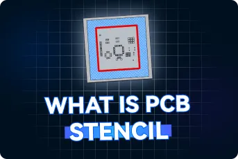
Solder stencils play a crucial role in modern PCB assembly, enabling precise application of solder paste to circuit boards for surface-mount components. These thin metal sheets, typically made from stainless steel or laser-cut foil, feature apertures that correspond to the pads on a PCB layout. By aligning the stencil over the board and spreading solder paste through it, engineers and hobbyists achieve uniform deposits, minimizing defects like bridging or insufficient solder that can lead to faulty connections. For anyone searching for information on solder stencils, this tag serves as a comprehensive resource covering design, fabrication, and usage techniques. Understanding the fundamentals starts with selecting the right thickness—usually between 0.1mm and 0.15mm for fine-pitch components—to ensure optimal paste release without smearing. Practical applications range from rapid prototyping in small-scale electronics projects to high-volume manufacturing, where stencils integrated with automated screen printers boost efficiency and yield rates. Best practices include proper cleaning to prevent residue buildup, using fiducial marks for accurate alignment, and incorporating aperture reductions for components prone to tombstoning. Whether you are troubleshooting common issues like paste misalignment or exploring advanced options such as frameless stencils for cost-effective setups, the articles gathered under this Solder Stencil tag offer detailed guides and real-world examples. Delving into these resources can help refine your assembly process, from DIY methods using etching kits to professional services for complex multilayer boards, ultimately leading to more reliable electronic designs.
Video Guide
-
00:51
Technical Articles
Nothing was found for this tag, try another tag
Get in Touch
Send Message
- Products & Service
- Company
- About AIVON
- Contact
- News
- Blog
- Certification
-


- Payment
-


2026 AIVON.COM All Rights Reserved