Vias Look Simple — But They Control PCB Yield
WHAT THIS VIDEO COVERS
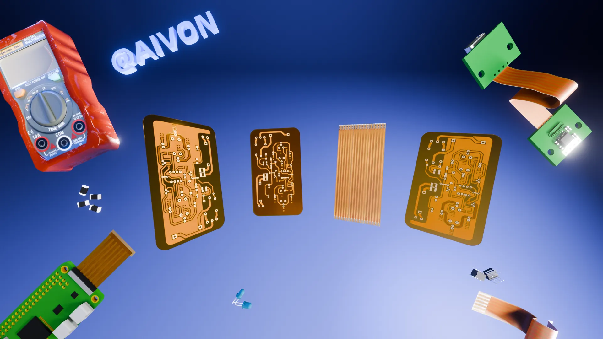
Vias may appear simple in your PCB layout software, but they significantly influence fabrication cost, assembly success, and long-term product reliability. This video reveals practical via design guidelines that separate high-yield boards from problematic ones.
The content covers the risks of overusing tiny vias, which increase drilling complexity, tooling costs, and reduce structural integrity over time. It explains the critical importance of respecting aspect ratio — especially on thicker boards — to ensure consistent plating and prevent thin copper walls that lead to failures. Viewers learn the proper handling of via-in-pad designs, including filling and capping requirements to avoid solder wicking and weak joints during SMT assembly.
Additional emphasis is placed on standardizing drill sizes to streamline production and control costs. These manufacturability principles apply to rigid PCB, HDI PCB, multilayer PCB, and high-frequency designs.
Whether developing PCB prototypes or scaling to mass production, thoughtful via decisions made early prevent costly revisions and improve overall board performance.
Get an instant PCB quote or explore HDI PCB capabilities and turnkey PCB assembly services.
KEY HIGHLIGHTS
- Via Size Matters: Avoid overusing tiny vias as they raise fabrication costs, complicate drilling, and reduce long-term mechanical reliability.
- Aspect Ratio Control: Maintain proper aspect ratio to ensure consistent plating; violations on thick boards lead to thin copper walls and field failures.
- Via-in-Pad Risks: Without filling and capping, vias in pads cause solder wicking, weak joints, and assembly defects.
FAQ
Q1: Why do small vias increase PCB manufacturing costs?
A1: Tiny vias require smaller drills, more precise processes, and higher tooling costs while reducing yield and long-term reliability.
Q2: What is the risk of via-in-pad without proper treatment?
A2: Solder can wick into the hole during assembly, weakening solder joints, causing defects, and leading to reliability issues.
Q3: Why is standardizing drill sizes important in PCB design?
A3: Multiple drill sizes slow production, increase setup costs, and reduce overall manufacturing efficiency. Standardization improves yield and lowers pricing.
Vias Look Innocent on screen?
But in real life, they control cost, reliability, and yield.
Here are some must-know tips.
One. Don't overuse tiny vias.
Smaller isn't always better.
Tiny drills increase fabrication complexity,
raise tooling cost,
and reduce structural reliability over time.
Two. Respect aspect ratio.
When the board is thick and the hole is narrow,
plating becomes inconsistent.
Thin copper walls are where long-term failures begin.
Three. Be careful with via-in-pad.
Without proper filling and capping,
solder can wick into the hole,
weakening joints and creating assembly defects.
Four. Standardize drill sizes.
Too many drill variations slow production and increase cost.
Good hole design isn't about routing freedom.
It's about manufacturability and controlled risk.