Analog-Driven SoC Design Choices: Balancing Analog and Digital in Advanced Nodes
Despite the semiconductor industry's shift toward digital dominance in the early 21st century, analog and mixed-signal circuits continue to play a vital role in System-on-Chip (SoC) designs. Scaling below 7nm has intensified demands for ultra-high-speed interfaces (e.g., 112 Gbps+ SerDes, HBM, LPDDR, and D2D links) in AI, high-performance computing (HPC), networking, and mobile applications. Purely digital implementations struggle with reduced supply voltages, power constraints, and the precision required for I/O, PLLs, DLLs, and sensors.
Advanced interfaces often favor analog-top or mixed-signal approaches to meet performance, power, and area targets.
Striking the Right Balance Between Analog and Digital
Modern applications impose stringent requirements on bandwidth, noise, and power efficiency. While digital logic excels at density and scalability, many real-world signals (sensor data, RF, high-speed links) benefit from analog preprocessing. Trade-offs must be evaluated early: analog provides superior noise performance and precision at the front-end, while digital handles complex processing and calibration.
Designers increasingly adopt hybrid architectures, leveraging analog for critical interfaces and digital for control and computation.
Key Challenges in Sub-7nm Analog Design
Low Supply Voltage: Voltages have dropped toward 0.7V and below, reducing transistor overdrive. Solutions include precharge techniques that set initial conditions for reliable low-voltage operation.

Variable Transconductance and Biasing: Shorter channels make gm less predictable. Analog designers use longer channels and higher VDS biasing (e.g., 3x overdrive) where digital flows default to minimum lengths.

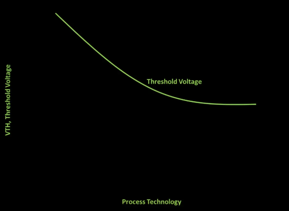
High Threshold Voltage (Vth): Vth now represents a larger fraction of supply voltage, limiting headroom. Custom pull-up/pull-down structures and careful device sizing help maintain performance.
Additional issues include increased mismatch, higher flicker noise, reduced gain, and greater sensitivity to process variation, crosstalk, and power integrity.
Implementation Strategies and Challenges
Digital Implementation
Relies heavily on automation scripts, APR tools, and standard cells. Challenges include achieving ultra-low skew (e.g., <50 ps for multi-Gbps links), managing EM/IR drop, and handling complex DRC in multi-patterning flows.
Analog and Mixed-Signal Strategies
- Custom layouts for parasitic control and matching.
- Accurate SI/PI simulation and 2.5D/3D system-level sign-off.
- Precharge architectures and alternative signal representations (e.g., time/delay-based instead of voltage).
- Hybrid approaches using digital blocks (switches, ring oscillators) for analog functions.
Close correlation between implementation and sign-off tools accelerates convergence.
The Necessity of Analog-Digital Interaction
Increased wiring density and complex architectures require seamless signal exchange between domains. Custom techniques help mitigate crosstalk while enabling higher speeds. Nanoscale transistors switch rapidly, opening opportunities to process analog information through digital-like structures.
Resurgence of Analog Techniques in Industry Applications
The proliferation of sensors in IoT, mobile, automotive, and industrial systems drives demand for power-efficient analog interfaces. Analog expertise is crucial for integrating diverse functions under tight constraints, influencing everything from edge AI to precision measurement.
Implications for PCB Design and Electronics Manufacturing
SoC-level analog decisions directly impact board-level design:
- High-Speed Interfaces: Require impedance-controlled routing, tight length matching, and low-noise power distribution on PCBs.
- Mixed-Signal Partitioning: Careful separation of analog and digital domains, grounding strategies, and decoupling to preserve signal integrity.
- System-Level Challenges: 2.5D/3D packaging and SiP demand advanced PCB fabrication capabilities, including HDI, controlled impedance, and thermal management.
- Reliability: Robust analog front-ends reduce system sensitivity to board-level parasitics, easing manufacturing tolerances in high-volume production.
PCB manufacturers supporting advanced SoCs must deliver precision stackups, tight tolerances, and high-reliability processes to complement sophisticated silicon designs.
FAQ
Q1: Why can't high-speed interfaces be implemented entirely in digital at advanced nodes?
A1: Reduced supply voltages and headroom limit digital circuit performance for precision timing, noise-sensitive functions, and ultra-high data rates.
Q2: What are the main challenges for analog in sub-7nm?
A2: Low voltage, high Vth relative to supply, increased mismatch, noise, and the need for custom layouts versus digital automation.
Q3: How does analog-driven design affect PCB development?
A3: It drives requirements for superior signal integrity, power integrity, and mixed-signal layout practices on the board to fully realize SoC performance.