Analog-to-digital converters (ADCs) form the critical interface between the analog world and digital processing on printed circuit boards. Achieving high accuracy and speed requires careful selection of conversion architecture, thorough understanding of error mechanisms, and disciplined PCB layout that minimizes parasitics, noise, and thermal gradients.
Fundamental ADC Conversion Principles and PCB Implications
All ADCs sample an analog input and quantize it into digital codes. The sampling process introduces aperture uncertainty and switch-related errors that directly depend on PCB trace inductance, capacitance, and grounding. On multilayer boards, maintaining low-impedance return paths and controlled-impedance routing for analog signals is essential to preserve signal integrity. Material selection—such as low-loss dielectrics and appropriate copper thickness—further influences high-frequency performance and long-term stability.
Common ADC Architectures and Their PCB Layout Requirements
Flash ADCs deliver the highest conversion speeds through parallel comparators. They demand extremely low-impedance power distribution and careful decoupling on the PCB to prevent supply noise from affecting multiple comparators simultaneously. Wide, short traces and dedicated power planes become mandatory at gigasample rates.
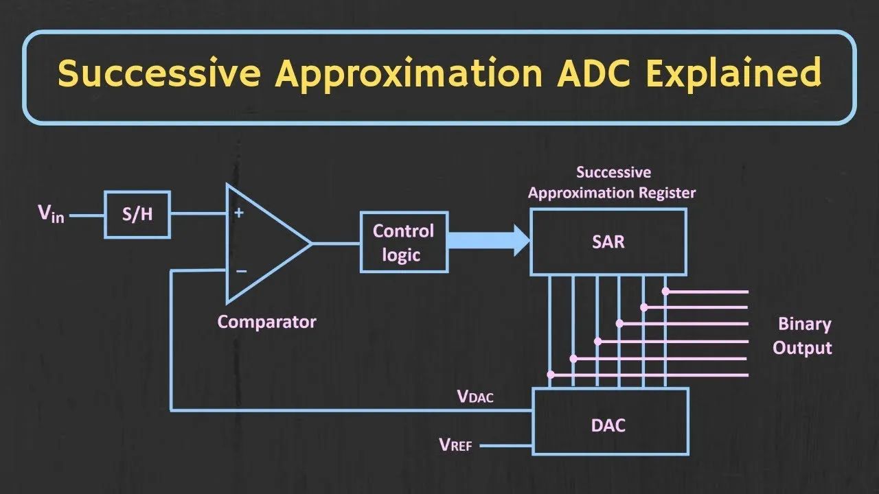
Successive Approximation Register (SAR) ADCs offer an excellent balance of speed, resolution, and power. Their internal capacitive DAC requires stable reference voltages; therefore, reference traces must be routed with minimal inductance and guarded against digital switching noise. SAR ADCs are particularly sensitive to reference settling time, making local bypassing and star-grounding techniques critical.
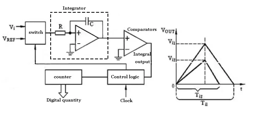
Dual-slope ADCs provide excellent noise rejection and linearity for low-to-medium speed applications. Their integrating nature benefits from low-leakage PCB materials and careful guard-ring placement around the integrator capacitor to minimize leakage currents and dielectric absorption effects.
Pipelined ADCs, including SHA-less architectures, achieve high throughput by staging multiple conversion steps. SHA-less designs reduce power but increase sensitivity to front-end settling and clock jitter. PCB layout must ensure matched propagation delays between analog and clock paths, often requiring controlled-impedance differential pairs and precise via placement.
Offset, Gain Errors, and Sampling Switch Limitations
Offset and gain errors shift the transfer function and scale the digital output. On the PCB these errors are aggravated by thermocouple effects at dissimilar metal junctions, thermal gradients across the board, and reference voltage drift caused by load changes. Self-calibration routines inside modern ADCs can correct many static errors, but they cannot compensate for layout-induced dynamic errors such as reference bounce or ground potential differences.


Sampling switch errors arise from charge injection, clock feedthrough, and on-resistance variation. Two primary sources are signal-dependent charge injection and finite switch resistance that interacts with external source impedance. PCB designers mitigate these by placing the ADC as close as possible to the signal source, using low-inductance vias, and ensuring the analog input trace is shielded or guarded to reduce external capacitance and noise pickup.

Calibration Techniques and Board-Level Implementation
Internal and self-calibration features in precision ADCs correct offset, gain, and linearity errors at power-up or periodically. Effective use requires stable power supplies and quiet digital interfaces during calibration cycles. On the HDI PCB, route calibration-related digital lines away from sensitive analog sections or use differential signaling with proper termination to prevent digital noise from corrupting the calibration process.

Five Practical Steps to Design an ADC Front-End on PCBs
- Define resolution, speed, and input range requirements while considering PCB noise floor and thermal environment.
- Select the ADC architecture and reference scheme, then plan local decoupling and reference routing.
- Design the input conditioning circuitry (buffers, filters, or attenuators) with attention to bandwidth, settling time, and impedance matching.

- Implement grounding and power distribution strategies—star grounding, separate analog/digital planes, and stitching vias—to minimize common-impedance coupling.
- Verify the complete signal chain through simulation of layout parasitics and prototype testing, iterating copper pours, via counts, and component placement as needed.
High-Speed Interface Considerations Between ADCs and DACs
In systems containing both ADCs and DACs, setup and hold times at the digital interface become critical. PCB trace length matching, controlled impedance, and proper termination prevent timing violations that degrade effective number of bits (ENOB). Short, symmetric routing between converter and FPGA or processor, combined with appropriate series termination resistors, ensures reliable data transfer at high clock rates.

PCB Layout Best Practices for ADC Circuits
- Place the ADC close to the analog signal source and reference components.
- Use dedicated analog ground planes with single-point connection to digital ground.
- Provide multiple low-ESL decoupling capacitors directly at power pins.
- Route analog traces on inner layers when possible or use guard traces on outer layers.
- Employ thermal vias under power-dissipating components to maintain uniform temperature across the ADC package.
- Specify low-loss PCB substrates and appropriate copper weights for high-speed or high-resolution designs.
Conclusion
Achieving the full specified performance of modern ADCs requires the seamless integration of architecture selection, error analysis, calibration strategy, and rigorous PCB design practices. By addressing sampling switch limitations, reference stability, thermal gradients, and high-speed interface timing at the board level, engineers deliver superior signal integrity, noise immunity, and long-term reliability. These considerations are critical in automotive sensor systems, industrial instrumentation, medical imaging, and high-speed communications equipment. Early collaboration with an experienced PCB manufacturer ensures that stack-up design, material selection, via implementation, and manufacturing processes fully support the demanding analog performance requirements throughout the product lifecycle.