Single-Ended vs. Differential Signaling
Single-ended signals use one conductor referenced to a ground plane. The signal represents the voltage difference between the trace and ground. This approach assumes matched ground potentials at driver and receiver.
Differential signals use a pair of traces carrying equal-amplitude, opposite-polarity signals. The receiver detects the voltage difference between them, providing greater tolerance to ground potential differences between source and receiver.
In AC or high-frequency operation, single-ended signals are more susceptible to ground bounce and noise due to parasitic inductance in the return path. Differential pairs are inherently more robust because common-mode disturbances (affecting both lines equally) are rejected at the receiver.
Differential signaling also offers superior immunity to external electromagnetic interference (EMI), as induced voltages appear as common-mode and largely cancel out.
Advantages and Disadvantages of Differential Signaling
Advantages:
- Reduced sensitivity to ground potential variations.
- Stronger noise immunity and lower EMI emissions due to field cancellation.
- Better support for bipolar signaling in single-supply systems.
Disadvantages:
- Requires tightly matched amplitude, phase (180 degree difference), and trace lengths.
- More sensitive to skew and impedance discontinuities than single-ended designs.
Essential Differential Pair Design Rules
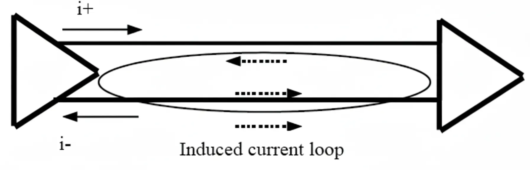
Tight Coupling: Equal and opposite currents generate canceling magnetic fields, reducing EMI. External noise appears as common-mode, which the receiver rejects.
Matched Lengths and Consistent Spacing: Maintain equal electrical lengths to prevent skew and ensure simultaneous transitions. Uniform spacing avoids impedance variations and unbalanced coupling.
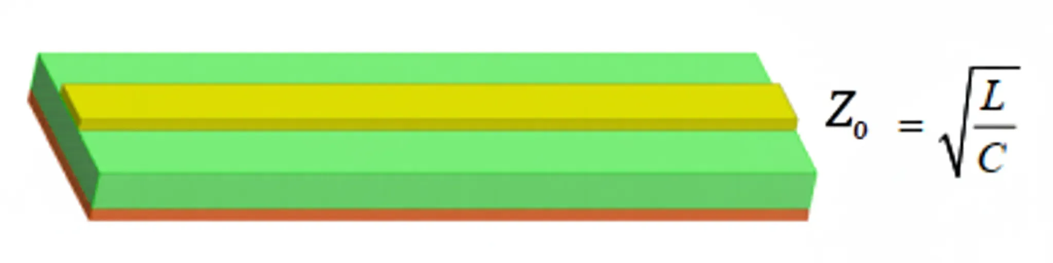
Controlled Impedance: Target consistent differential impedance (commonly 100 Ohm +/- 15%) through trace geometry, spacing, and dielectric properties. Avoid discontinuities that cause reflections.
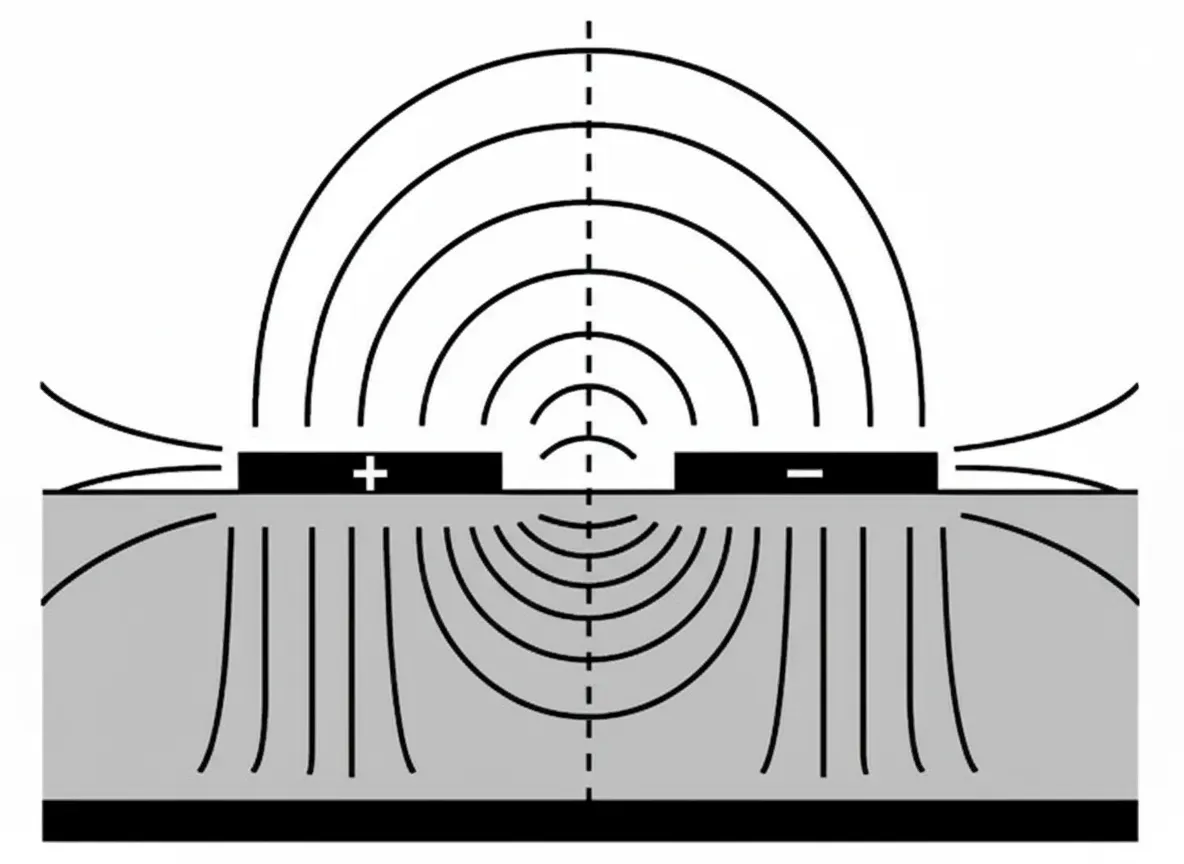
Return Path Integrity: Provide continuous, low-inductance return paths (typically adjacent ground planes) to minimize loop area and EMI. Layer changes or plane splits must be carefully managed.
In-Depth Analysis of Differential Signal Return Paths
A common misconception is that differential currents form a completely closed loop between the two traces with no return current in the reference plane. In reality, return currents do flow through the reference plane (similar to single-ended signals), but in an ideal differential pair, the equal-and-opposite currents and their returns produce canceling magnetic fields, resulting in very low net radiation.
When ground potentials differ or external fields are present, common-mode effects are minimized at the receiver, contributing to robust performance.
Design Approaches by Layer Count
Multi-Layer Boards
Route differential pairs adjacent to a continuous ground or power plane. This provides the shortest return path, minimal loop area, and excellent field cancellation.
Two-Layer Boards
More challenging due to limited layers. Common strategies include:
- Routing pairs on one layer with ground pours or traces on both sides as returns.
- Maintaining a solid reference plane on the opposite layer beneath the pair.
- Cross-routing (top/bottom) with careful via stitching and ground trace continuity.
Key Challenges on Two-Layer Designs
- Preserving reference plane integrity under the pair.
- Managing layer transitions for both signals and returns.
- Ensuring low-impedance connections via ground vias.
- Minimizing length mismatches in both signal pairs and return paths.
Proper via placement, stitching, and avoidance of splits are critical to prevent uncontrolled return currents that increase EMI or degrade signal quality.
PCB Manufacturing and Design Considerations for Differential Signals
Achieving high-performance differential routing requires close collaboration between design and manufacturing:
- Impedance Control: Precise dielectric thickness, trace width/spacing, and material selection (e.g., low-loss laminates) are essential. Tight tolerances demand advanced fabrication capabilities.
- Stackup Optimization: Symmetric stackups and reference plane placement minimize warpage and support consistent impedance.
- Signal Integrity Enhancements: Controlled etching, surface finish quality, and registration accuracy reduce discontinuities.
- Testing and Validation: Time-domain reflectometry (TDR) and insertion loss measurements verify performance.
For applications in automotive, industrial control, telecommunications, and high-speed computing, robust differential signaling directly impacts system reliability and EMC compliance.
Industry Trends
As data rates increase (e.g., PCIe, Ethernet, SerDes), emphasis on return path optimization, crosstalk mitigation, and advanced simulation grows. Tools for 3D electromagnetic modeling and automated constraint-driven routing help designers meet stringent requirements efficiently.
Frequently Asked Questions
Q1: Do differential signals eliminate the need for a ground plane?
A1: No. While differential pairs offer better noise immunity, a continuous low-impedance return path (ground plane) remains essential for minimizing EMI and maintaining signal integrity.
Q2: What is the most critical rule for differential pairs?
A2: Maintaining tight coupling, matched lengths, consistent spacing, and a continuous return path to control impedance and field cancellation.
Q3: Why is return path continuity important even for differential signals?
A3: Discontinuities force return currents to take longer paths, increasing loop area, EMI radiation, and potential common-mode conversion that degrades performance.