Background and Evolution of Analog IC Layout
Analog integrated circuit (IC) layout has historically been labor-intensive and highly manual due to stringent matching, symmetry, and parasitic control requirements. Unlike digital designs, analog circuits demand precise attention to device geometry, interconnect balancing, and process variation mitigation to achieve target performance, noise immunity, and offset cancellation.
Advances in Electronic Design Automation (EDA) tools now enable significant automation for analog layouts. Modern solutions can recognize schematic structures such as differential pairs and current mirrors, then generate multiple DRC-clean layout options that respect critical constraints - dramatically shortening the traditional iterative handoff between circuit designers and layout engineers.
Critical Requirements for Matched Differential Pair Layouts
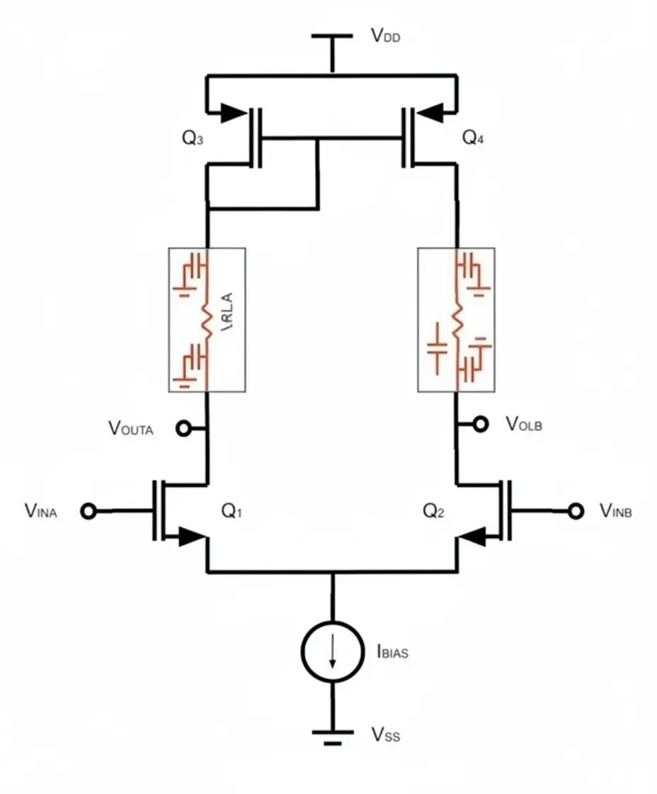
Differential pairs form the foundation of many analog building blocks, including operational amplifiers and comparators. Key layout requirements include:
- Device Matching: Identical W/L dimensions and orientation for paired transistors.
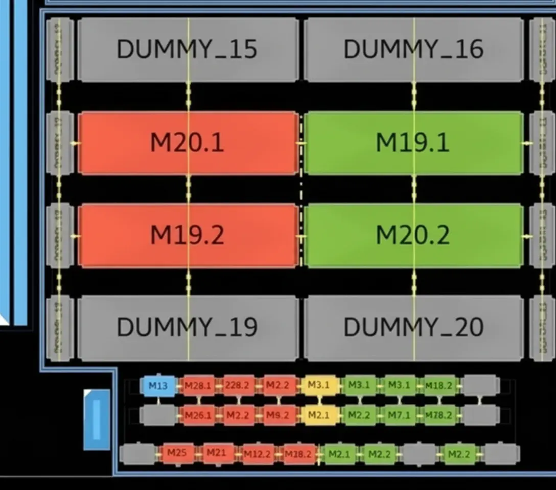
- Common-Centroid Arrangements: Placement that averages out process gradients (e.g., oxide thickness, doping variations) across the die.
- Symmetric Interconnects: Balanced parasitic resistance and capacitance on signal paths to minimize offset and improve common-mode rejection.
- Current Mirror Optimization: Minimal parasitic RC effects while maintaining matching.
These constraints directly impact parameters like input offset voltage, gain, and linearity.
How Automated Tools Streamline Analog Layout
Advanced EDA plugins (such as those integrated with Cadence Virtuoso) automatically detect schematic elements like differential pairs and current mirrors. The tool then applies expert-level constraints to generate multiple valid layout topologies quickly. Designers can evaluate options based on area, aspect ratio, and performance metrics without manual drafting.
Key Features Demonstrated in Typical Workflows
- Hierarchy and Cross-Probing: Schematic-to-layout linking allows instant visualization of how devices map to physical implementations.
- Common-Centroid Generation: Automatic row/column placement with consistent polygon orientation for matched devices.
- Symmetry Controls: Options to add dummy structures or enforce mirrored/butterfly layouts for enhanced gradient cancellation.
- Routing Analysis: Layer isolation views confirm balanced metal routing (M1-M5) for source/drain and interconnect nodes.
- Constraint Management: Schematic-driven rules ensure compliance with matching, proximity, and symmetry requirements.
For current mirrors connected to differential pairs, automation ensures symmetric routing and minimized parasitics, with options for mirrored or butterfly configurations.
Benefits Over Traditional Manual Flows
Traditional analog design flows involve schematic annotation, manual layout implementation, and multiple review iterations to verify symmetry and matching. Automated techniques compress this into minutes, enabling rapid exploration of design alternatives while maintaining or improving quality.
This productivity gain is especially valuable in competitive markets requiring fast time-to-market for mixed-signal SoCs, sensor interfaces, power management ICs, and RF/analog front-ends.
Relevance to PCB Design and Electronics Manufacturing
While automated IC layout occurs at the silicon level, it has downstream implications for PCB and system design:
- Mixed-Signal Integration: Well-matched analog ICs reduce sensitivity to board-level parasitics, simplifying high-speed or precision PCB layouts.
- Signal Integrity: Balanced on-chip routing complements careful PCB trace matching, impedance control, and grounding strategies in analog signal chains.
- High-Reliability Systems: In automotive, industrial control, medical, and aerospace applications, robust analog ICs (enabled by better layout) translate to more forgiving PCB assembly and higher overall system reliability.
- Design-for-Manufacturability (DFM): Understanding IC-level constraints helps PCB designers optimize land patterns, decoupling, and thermal management for analog components.
PCB manufacturers supporting advanced electronics benefit from customers using sophisticated EDA tools, as it leads to more mature designs with fewer revisions.
Industry Trends
The push toward greater analog automation continues with AI-assisted placement, machine learning for parasitic prediction, and tighter integration between schematic, layout, and verification environments. These tools help bridge the analog-digital design gap in complex SoCs while addressing challenges like process variation at advanced nodes.
FAQ
Q1: What is common-centroid layout and why is it important?
A1: A technique placing matched devices symmetrically around a common center to average process gradients, reducing mismatch in differential pairs and current mirrors.
Q2: How does automation benefit analog IC design?
A2: It generates multiple DRC-clean, constraint-aware layouts rapidly, allowing designers to evaluate trade-offs in area, parasitics, and symmetry much faster than manual methods.
Q3: Does automated analog layout eliminate the need for manual review?
A3: No - automation accelerates initial generation and exploration, but expert review remains essential for final optimization and application-specific nuances.