Rectifier circuits form the foundation of AC-to-DC conversion in power supply systems integrated on printed circuit boards. In PCB manufacturing and design, engineers must address not only circuit topology but also layout constraints, thermal dissipation, signal integrity, EMI/EMC compliance, and component reliability under real-world operating conditions. Proper PCB implementation of rectifiers and protection devices such as varistors directly impacts efficiency, ripple performance, long-term reliability, and manufacturing yield.
Common Rectifier Circuit Types and Their PCB Implications
Three primary rectifier topologies dominate power electronics applications: single-phase half-wave, single-phase full-wave (typically bridge), and three-phase rectifiers.
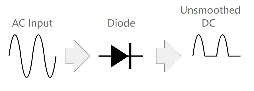
Single-phase half-wave rectification uses one diode to pass only one half-cycle of the AC waveform. While simple and low-cost, this approach produces significant ripple and lower efficiency. On a PCB, the long intervals between output peaks complicate filtering capacitor placement and increase the required board area for effective smoothing. Layout must minimize loop inductance to reduce voltage spikes during diode switching. For compact consumer electronics and IoT devices, designers may adopt an HDI PCB structure to reduce footprint while maintaining adequate signal and power routing density.
Single-phase full-wave rectification, commonly implemented with a four-diode bridge, converts both positive and negative half-cycles into unidirectional pulsating DC. Bridge rectifiers eliminate the need for a center-tapped transformer, reducing cost and complexity. In PCB terms, the bridge configuration requires careful routing of AC and DC paths to balance current distribution and minimize electromagnetic interference. Two diode forward drops occur during conduction, so thermal management becomes critical—designers often use thicker copper layers (2–3 oz or more) or thermal vias to dissipate heat from the diodes.
Three-phase rectifiers, using six diodes or thyristors, deliver higher power with inherently lower ripple. These are prevalent in industrial and high-power applications. PCB implementation demands robust power planes, multiple vias for high-current paths, and symmetrical layout across phases to maintain balance and prevent localized heating.
Diode Fundamentals, Selection, and Fast-Recovery Considerations
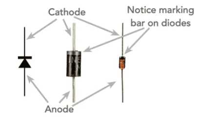
Rectifier diodes exploit the unidirectional conduction of a PN junction. Forward voltage drop typically ranges from 0.6–0.7 V for silicon diodes and lower (0.2–0.3 V) for Schottky types. Reverse leakage remains minimal until breakdown voltage is exceeded.
When selecting diodes for PCB designs, key parameters include:
- Peak reverse voltage rating exceeding the maximum expected AC peak plus margin.
- Forward current rating matching or exceeding load requirements.
- Forward voltage drop affecting overall efficiency and heat generation.
- Recovery time, especially important in high-frequency or switch-mode power supplies.
Standard rectifier diodes suit low- to medium-frequency applications but exhibit longer reverse recovery times. Fast-recovery diodes reduce turn-off time to microseconds or less, minimizing switching losses and improving efficiency in high-frequency circuits.
On PCBs, fast-recovery diodes help reduce EMI generated by abrupt current changes; however, their lower forward voltage and higher leakage require optimized layout to avoid parasitic effects. Package selection—through-hole, surface-mount, or bridge modules—directly influences thermal performance and automated assembly compatibility. High-power diodes often need bolt-on or heatsink-compatible packages with adequate copper pours and thermal vias on the PCB.
Precision Full-Wave Rectification Using Op-Amps
Standard diode bridges introduce two forward voltage drops and are unsuitable for precision low-level signal rectification. Op-amp-based precision rectifiers overcome diode threshold limitations by placing the diode within the feedback loop, achieving near-ideal rectification even for millivolt-level signals.
A common precision full-wave topology combines a precision half-wave rectifier with a summing amplifier. The circuit arranges diodes and resistors such that both positive and negative input peaks produce a unidirectional output with high accuracy and low ripple.
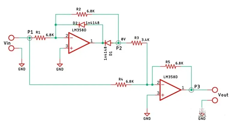 On a PCB, this demands:
- Low-offset, low-noise op-amps.
- Matched resistors for accurate gain settings.
- Careful grounding and decoupling to prevent noise coupling.
- Short trace lengths to minimize parasitic capacitance and inductance that can cause distortion.
Distortion sources include diode nonlinearity, temperature-induced threshold shifts, and power supply ripple. PCB designers mitigate these through star grounding, proper decoupling capacitor placement, and thermal isolation of sensitive analog sections from power components.
Varistor Integration for Overvoltage Protection
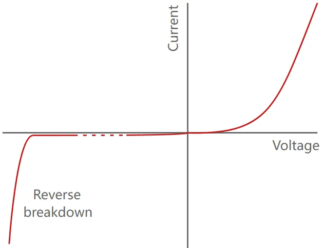
Varistors (voltage-dependent resistors, typically zinc-oxide based) provide essential surge protection in rectifier input stages. At normal operating voltages they exhibit high resistance and negligible leakage. When voltage exceeds the clamping threshold, resistance drops sharply, diverting surge energy and protecting downstream components.
Common failure symptoms include loss of clamping action, increased leakage, visible charring or cracking, and resistance drift. On PCBs, varistors must be placed close to the input connector or rectifier stage with short, wide traces to minimize inductance in the protection path. Series fuses or current-limiting resistors are often added to prevent varistor failure from causing catastrophic short circuits.
Varistors complement rectifier circuits by absorbing transients from switching noise, lightning, or inductive loads. In PCB stack-up design, placing varistors on outer layers with adequate creepage and clearance distances supports high-voltage isolation requirements.
PCB Design and Manufacturing Best Practices
Effective rectifier and protection circuit implementation on PCBs requires attention to:
- Copper thickness and trace width — sized for continuous and surge currents while managing temperature rise.
- Thermal management — copper pours, thermal vias, and heatsink mounting for diodes and varistors.
- Stack-up and material selection — higher Tg laminates or thicker copper for power applications; controlled impedance where high-frequency content exists.
- EMI/EMC mitigation — minimized loop areas, proper grounding planes, and shielding considerations.
- Component placement — input protection devices near connectors, rectifier diodes grouped for balanced current sharing, and sensitive precision sections isolated from power switching.
- Via design — multiple vias in parallel for high-current paths and thermal transfer.
- Reliability testing — accounting for thermal cycling, surge withstand, and long-term leakage in harsh environments.
By integrating these considerations early in the design phase, engineers achieve higher efficiency, lower ripple, improved surge immunity, and better manufacturability. Aivon’s PCB manufacturing capabilities support optimized stack-ups, heavy copper, and precise via structures required for demanding rectifier and protection circuits across automotive, industrial, telecom, and power supply applications.
Conclusion
Effective integration of rectifier circuits and varistor-based overvoltage protection is essential for reliable PCB-level power conversion. By addressing layout constraints, thermal dissipation, component selection, and manufacturing parameters from the earliest design stages, engineers can achieve superior efficiency, reduced EMI, and extended product lifespan. Whether applied in industrial power systems, precision instrumentation, or high-reliability automotive electronics, optimized PCB implementation of these circuits delivers measurable performance gains while supporting scalable, high-yield production.