Selecting the right MOSFET and implementing it correctly on a printed circuit board determines the difference between reliable operation and premature failure in power electronics. Engineers must evaluate datasheet parameters, thermal behavior, switching characteristics, and parasitic effects while simultaneously addressing PCB layout constraints such as trace inductance, thermal vias, copper thickness, and grounding strategies.
Key MOSFET Datasheet Parameters and PCB Implications
Manufacturers publish parameters that directly affect board-level performance. Key values include:
- VDS (Drain-Source Voltage): Maximum blocking voltage; derate for PCB voltage spikes caused by layout inductance.
- ID (Continuous Drain Current): Limited by package and PCB copper cross-section; requires adequate trace width and thermal relief.
- RDS(on): On-state resistance that generates heat; lower values demand thicker copper layers or more copper pours.
- Qg (Total Gate Charge) and Qg(th): Drive energy requirements that influence gate driver sizing and PCB trace routing for fast, clean switching.
- Ciss, Coss, Crss: Input, output, and reverse transfer capacitances that contribute to switching losses and potential ringing on the board.
- VGS(th) and gm (Transconductance): Threshold and gain characteristics that affect drive voltage margins and stability.

Parasitic capacitances calculated from datasheet values must be compared with PCB layout parasitics. Trace-to-ground capacitance, via capacitance, and coupling between adjacent traces can exceed device parasitics at high frequencies, degrading performance.
Ten Practical Rules for MOSFET Selection in PCB Designs
- Match VDS rating to the maximum expected voltage including PCB-induced ringing.
- Verify ID capability against both steady-state and peak currents while accounting for PCB copper heating.
- Prioritize low RDS(on) but balance against higher gate charge that increases driver power and layout complexity.
- Ensure adequate SOA (Safe Operating Area) margin for transient events common in switched-mode circuits.
- Select devices with appropriate gate threshold for the available drive voltage on the board.
- Consider package thermal resistance and plan corresponding PCB heatsinking (copper pours, thermal vias, heatsink attachment).
- Evaluate switching speed against EMI and layout constraints; faster devices require shorter gate loops.
- Check avalanche energy rating when inductive loads are present on the copper core PCB.
- Verify compatibility with the chosen gate driver topology and its PCB placement.
- Account for temperature derating across the full operating range of the assembled board.
Common MOSFET Failure Mechanisms and PCB-Level Prevention
MOSFETs fail through overvoltage, overcurrent, thermal runaway, gate oxide breakdown, and parasitic turn-on. On the PCB these manifest as:
- Excessive trace inductance causing voltage spikes → mitigate with short, wide traces and snubber networks.
- Inadequate thermal dissipation → use multiple thermal vias under the drain pad, thicker copper, and proper copper pour design.
- Gate drive issues leading to partial turn-on → ensure low-inductance gate return paths and proper decoupling.
- Miller capacitance effects causing unintended turn-on during fast dv/dt → add gate-to-source resistors or use negative gate drive where layout allows.
Low-power BLDC motor applications are especially sensitive to these issues because of high switching frequencies and compact board layouts. Smoking within seconds under load typically indicates either insufficient heatsinking on the PCB or gate drive that fails to keep the device fully enhanced.
Gate Driver Topologies and PCB Implementation
Common driver configurations include direct drive, totem-pole, bootstrap, and isolated drivers. Each imposes specific layout rules:
- Keep gate and source return traces as short and wide as possible to minimize inductance.
- Place driver IC close to the MOSFET to reduce loop area.
- Use separate analog and power ground planes connected at a single point when both exist on the board.
- Provide local decoupling capacitors with low-ESL routing.
Bootstrap drivers require careful diode and capacitor placement to avoid bootstrap supply droop during high-side switching.
BJT versus MOSFET Comparison for PCB Applications
Bipolar junction transistors offer high current gain in some configurations but require continuous base current, leading to higher drive losses.


MOSFETs provide voltage-controlled operation with negligible gate current after charging, making them preferable for high-frequency switching on PCBs.


Darlington pairs combine high current gain with the simplicity of a single base drive but introduce higher saturation voltage and slower switching.

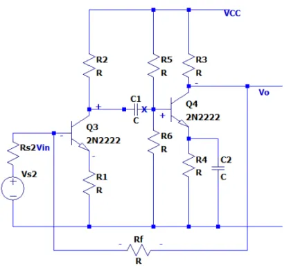
Common-emitter, common-base, and emitter-follower stages each present different input/output impedance and stability requirements that influence PCB grounding and feedback routing.

When high current gain with low drive power is needed, Darlington configurations can be used, but thermal management becomes critical because of the compounded VCE(sat) drop.
Practical PCB Design Practices
- Route gate traces away from drain and source switching nodes to reduce capacitive coupling.
- Use controlled-impedance stack-ups for high-speed gate signals.
- Implement star grounding or ground planes with stitching vias around power stages.
- Simulate layout parasitics early to predict switching behavior before fabrication.
- Specify appropriate surface finish and solder mask for high-current or high-frequency boards.
By integrating device selection, failure-mode analysis, and PCB layout rules from the earliest design stage, engineers achieve higher reliability, lower EMI, and improved manufacturing yield across automotive, industrial, and consumer power applications.
Conclusion
Successful MOSFET selection and long-term reliability in power electronics ultimately depend on integrating device parameters with disciplined PCB design and manufacturing practices. By applying the ten selection rules, mitigating common failure modes through optimized layout, and addressing thermal, inductive, and gate-drive constraints at the board level, engineers achieve higher efficiency, lower EMI, and improved production yields. These principles are essential in automotive power systems, industrial motor drives, renewable energy converters, and high-density consumer electronics. Early collaboration with an experienced PCB manufacturer helps ensure that stack-up, copper weight, via design, and material choices fully support the intended electrical and thermal performance throughout the product lifecycle.