Introduction
In analog circuit design, the choice between differential and single-ended amplifiers significantly impacts system performance, particularly in noisy or high-precision environments. Differential amplifiers excel at rejecting common-mode noise while amplifying the desired signal difference, making them indispensable in sensor interfaces, data acquisition, medical instrumentation, and industrial control systems. For PCB manufacturers and electronics engineers, understanding these advantages guides optimal layout practices, component selection, and production strategies to achieve high common-mode rejection ratio (CMRR) and signal integrity.
Common-Mode Noise in Single-Ended Circuits
Single-ended amplifiers reference the signal to ground or a fixed supply rail. Any noise present on the supply, ground, or coupled through the load appears directly in the output as interference. This common-mode noise introduces spurious frequency components and degrades overall accuracy, especially when amplifying small signals from distant sensors or over long cables.
Differential pairs address this limitation by processing signals as the difference between two complementary paths, effectively canceling common-mode components while reinforcing the differential signal.
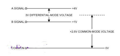
Common-Mode Level and Differential Signals
The common-mode level (CM) represents the average voltage present on both signal lines relative to a reference. The differential signal is simply the voltage difference between the two lines (V2 - V1). Effective differential designs maintain stable operation across varying common-mode levels while providing high gain for the differential component.
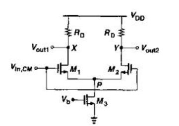
Tailed Differential Pair and Constant Tail Current
Practical differential amplifiers often incorporate a tail current source connected to the common emitter (BJT) or source (MOS) node. This constant current ensures symmetric branch currents regardless of input signal or common-mode variations.
Key Benefits:
- Stabilizes transistor operating points
- Improves output linearity
- Enhances rejection of common-mode interference
- Simplifies bias design across a wide input range
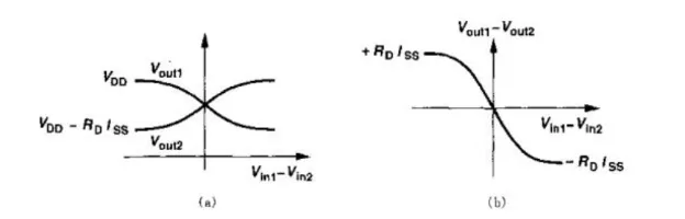
Input-Output Characteristics
The differential transfer characteristic shows maximum small-signal gain when inputs are balanced (Vin1 approx Vin2). The output swing is limited by supply rails and load conditions. With proper biasing, small differential inputs are amplified linearly while common-mode signals are strongly attenuated - resulting in superior CMRR compared to single-ended topologies.
Summary of Key Advantages
Superior Common-Mode Noise Rejection: Differential amplifiers subtract inverted signals, canceling noise that appears equally on both inputs.
Improved Bias Stability: The tail current source makes performance largely independent of common-mode voltage variations.
Better Linearity and Dynamic Range: Enhanced rejection of interference leads to cleaner output signals.
Suitability for Balanced Transmission: Ideal for long-distance sensor connections and environments with significant electromagnetic interference.
Trade-offs include increased circuit complexity, silicon area, and power consumption compared to single-ended designs. It also requires careful matching of components for optimal CMRR.
PCB Design and Electronics Manufacturing Considerations
Achieving the full benefits of differential amplifiers in production hardware demands disciplined PCB practices:
- Symmetrical Layout and Matching: Place matched resistor networks or transistor pairs symmetrically. Minimize trace length differences in differential pairs to preserve CMRR and reduce phase errors.
- Grounding and Partitioning: Implement a solid analog ground plane with star grounding or careful analog/digital separation. Avoid ground loops that can introduce common-mode noise.
- Signal Integrity: Route differential pairs as tightly coupled traces with controlled impedance. Use guard rings around high-impedance nodes and shielding for sensitive inputs.
- Power Integrity and Decoupling: Provide clean, low-noise power rails with close-proximity decoupling capacitors to prevent supply noise from degrading performance.
- Thermal Considerations: Minimize thermal gradients across matched components to reduce offset drift and maintain long-term stability.
- Manufacturing Best Practices: Precision assembly with matched component groups, thorough cleaning, and functional testing of CMRR/gain are essential. Multilayer boards with dedicated analog planes support high-performance implementations.
Industry Applications and Trends
Differential amplifiers dominate in precision measurement, audio, communications, and industrial sensor conditioning. Modern trends include higher integration (e.g., in instrumentation amplifiers), lower power for portable devices, and combined use with high-resolution ADCs in mixed-signal systems.
Supporting Precision Analog Design Through PCB Manufacturing
The advantages of differential over single-ended architectures are fully realized only with excellent PCB fabrication and assembly. Expertise in analog layout, precision matching, low-noise design, and reliable manufacturing processes enables OEMs to deliver high-accuracy, noise-immune analog front-ends for demanding applications.
FAQs
Q1: Why do differential amplifiers reject common-mode noise better than single-ended circuits?
A1: They amplify only the difference between two signals while subtracting identical (common-mode) components, significantly reducing interference from power supplies, ground, or external coupling.
Q2: What is the role of the tail current source in a differential pair?
A2: It stabilizes bias currents, improves linearity, and makes performance less sensitive to common-mode voltage variations.
Q3: How does PCB layout affect differential amplifier performance?
A3: Proper symmetrical layout, matched routing, solid grounding, and noise isolation are critical to maintaining high CMRR, low offset, and overall signal fidelity.