Overview
Differential operational amplifier circuits effectively suppress common-mode signals while amplifying only the differential component. This property makes them widely used in voltage sensing and signal conditioning applications.
Circuit Configuration
The following diagram shows a typical differential circuit.
Target measured voltage refers to the voltage to be acquired and processed, for example bus voltage or AC voltage measurements. Differential divider resistors on the non-inverting and inverting branches scale high-voltage signals down to levels suitable for the op amp, producing Vin+ and Vin-.
Feedback: for an op amp to operate in the linear region it must use negative feedback. Without feedback (open-loop) or with positive feedback, the circuit behaves as a comparator rather than an amplifier; the op amp then operates in saturation or a nonlinear region and the output approaches the supply rails.
The circuit below illustrates positive feedback. In this configuration the op amp cannot be treated as a linear amplifier; with large open-loop gain it becomes a hysteresis comparator and operates in the nonlinear or saturated region.
The following is also a comparator structure. Because the op amp open-loop gain is very large, without negative feedback it functions as a voltage comparator rather than a linear amplifier.
If the feedback resistor connects the output to the inverting input (-), that is negative feedback and the circuit amplifies signals while the output remains within the supply range. If the resistor connects to the non-inverting input (+), that is positive feedback and the circuit functions as a comparator.
In practice it is preferable to use dedicated comparators such as LM339, LM393, or LM211 instead of repurposing op amps as comparators, because internal operating conditions differ between comparators and op amps.
Comparators often include series current-limiting resistors (for example R74 and R77) because during rapid output transitions charging and discharging of capacitive loads produces current spikes. The resistors limit these currents to protect the devices.
RC filtering may be applied to prevent output overshoot and reduce signal distortion.
Calculating the Differential Input Voltage
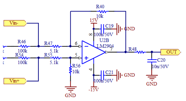
Consider the circuit below with specified resistor values for calculation. A common characteristic of differential circuits is symmetry: for example R40 = R56 and R47 = R55, so the two divider branches are equal.
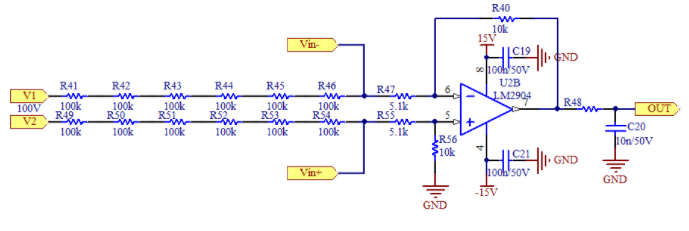
How are Vin+ and Vin- calculated? First derive them using full voltage-division analysis, then simplify. Using the virtual short property between the op amp inputs, and noting the coefficient 6 refers to six 100k resistors used to simplify the expressions, the node voltages can be written and solved by standard divider formulas.
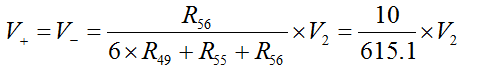
Apply voltage-division to obtain Vin+:
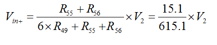
Similarly, compute Vin- by voltage division:
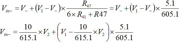
Subtracting gives Vin+ minus Vin-. A simpler approach uses the virtual short to form an equivalent divider network:
Using that simple divider, the differential input voltage calculation reduces to a single division, yielding:
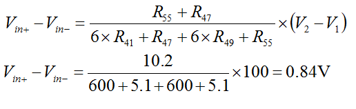
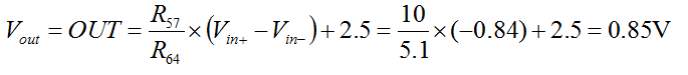
The resulting differential input voltage in this example is 0.84 V.
Differential Amplifier Calculation
The gain derivation continues to follow the virtual short and virtual open assumptions. When R56 = R40 and R47 = R55, the differential gain expression simplifies as shown:
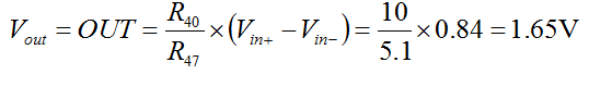
In practical designs, choosing equal resistor ratios on both branches simplifies calculation and implementation.
Offset Calculation for the Amplifier
Why offset the output? Data acquisition ICs and MCUs typically cannot sample negative voltages, so the amplifier output is shifted upward to ensure it remains positive.
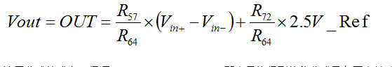
In the offset circuit, instead of tying the non-inverting input resistor to ground, apply an offset voltage (reference). Using superposition, the final expression is obtained provided resistor pairs satisfy R64 = R72 and R73 = R57. The offset simply adds a voltage term, for example a 2.5 V reference, to the original output expression.
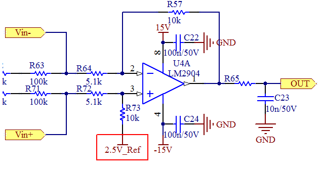
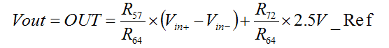
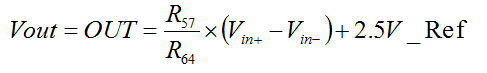
Choosing an appropriate offset value ensures the amplifier output is always positive.
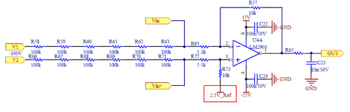
For example, if the input becomes -100 V in the example circuit, the offset produces a positive output so the signal meets MCU input requirements:
Offset circuits are commonly used when measuring AC signals or negative DC voltages in control and measurement systems to ensure compatibility with data acquisition hardware.