Introduction
The differential amplifier is a foundational building block in analog electronics. It amplifies the difference between two input signals while rejecting common-mode noise, making it essential for sensor interfaces, instrumentation, data acquisition systems, and operational amplifier input stages. For electronics engineers and PCB manufacturers, mastering differential amplifier design is critical for achieving high common-mode rejection ratio (CMRR), low noise, and reliable performance in real-world mixed-signal environments.
Differential Amplifier Overview
A differential amplifier produces an output proportional to the voltage difference between its two inputs. It offers significant advantages over single-ended amplifiers, including better noise rejection, improved dynamic range, and suitability for balanced signal transmission over long distances.
Two primary implementations are widely used:
- BJT (Bipolar Junction Transistor) differential pairs - common in discrete or integrated circuit front-ends.
- Op-amp-based differential circuits - flexible and widely used in precision applications.
BJT Differential Amplifier
Circuit Description
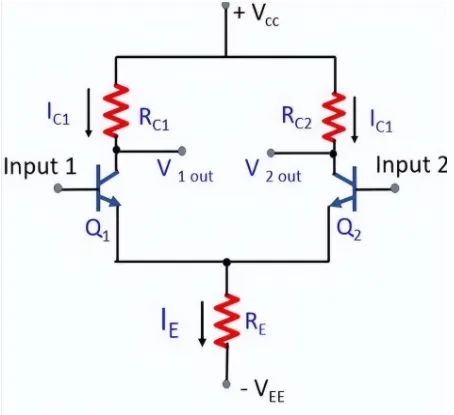
A classic BJT differential pair consists of two matched transistors (Q1 and Q2) with emitters connected to a common current source or resistor (Re). Collectors connect to load resistors (RC) tied to the positive supply. Inputs are applied to the bases, and outputs are taken from the collectors. The circuit can operate from dual or single supplies.
Four Common Configurations
- Dual input, balanced output
- Dual input, single-ended output
- Single input, balanced output
- Single input, single-ended output
Differential Operation
When a positive signal is applied to Q1 (Q2 base grounded or constant), Q1 conducts more, lowering its collector voltage (inverted output) while increasing emitter current. This raises the common emitter voltage, reducing Q2 conduction and raising Q2's collector voltage (non-inverted output). The complementary behavior produces a high-gain differential signal. Matched transistor characteristics and a stable tail current are essential for high CMRR.
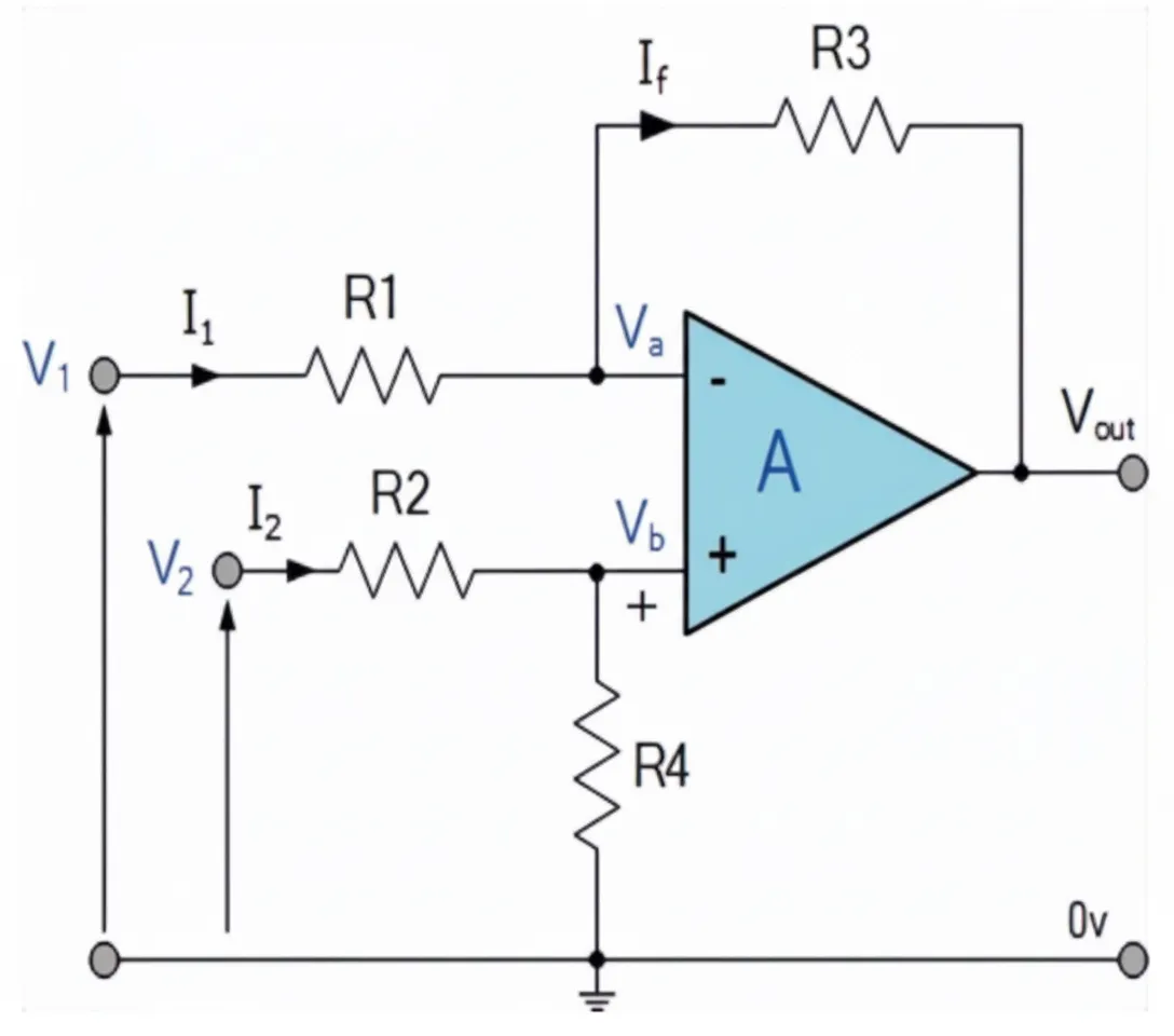
Op-Amp Based Differential Amplifier
Basic Circuit and Transfer Function
The standard four-resistor differential amplifier uses one op-amp with resistors R1/R2 on the inverting input and R3/R4 on the non-inverting input. Using superposition, the output voltage is:
Vout = (R2/R1) * (V2 - V1) (when R1 = R2 and R3 = R4)
For unity gain (R1 = R2 = R3 = R4), the circuit simplifies to:
Vout = V2 - V1
This configuration provides good performance but has relatively low input impedance.
Practical Applications and Examples
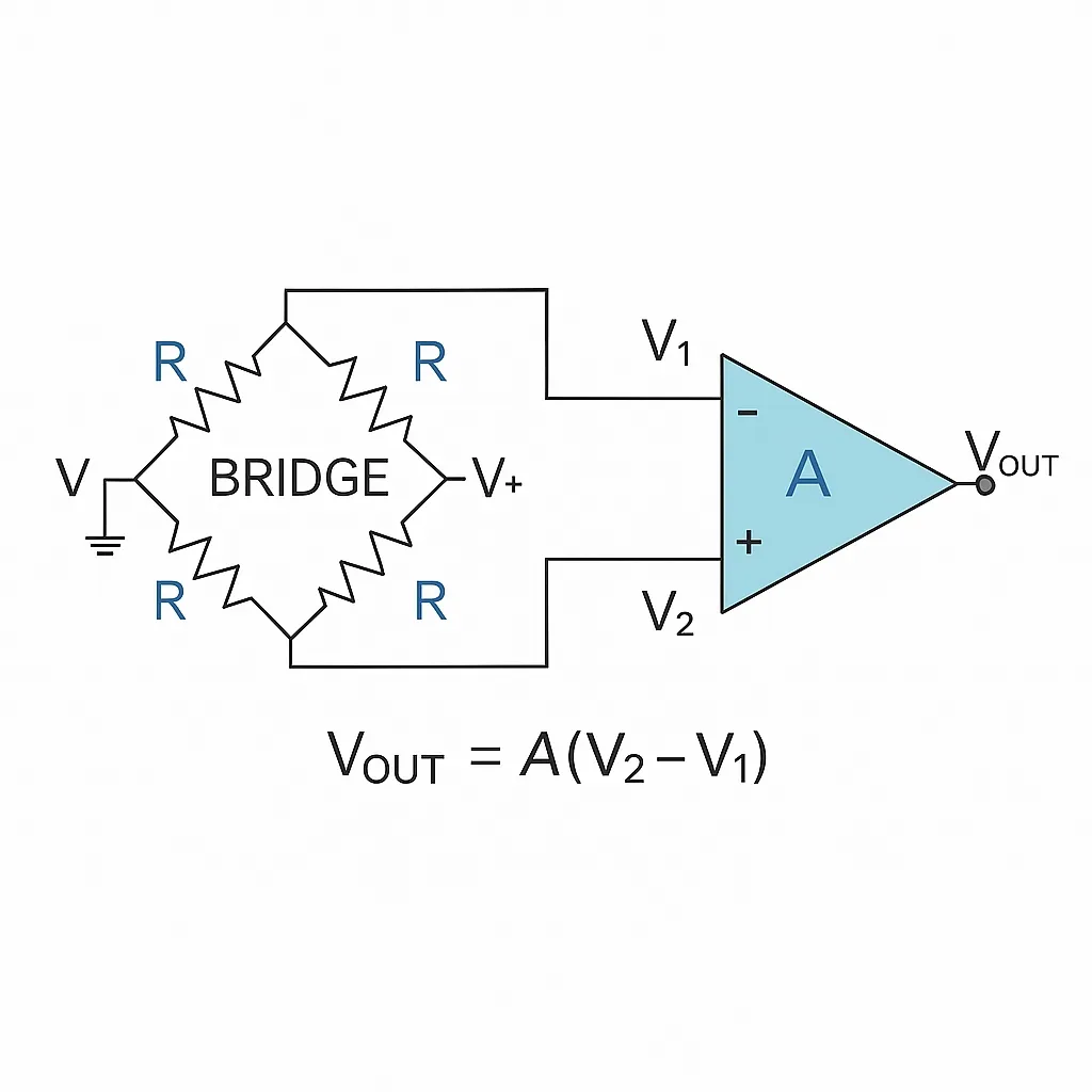
Wheatstone Bridge Interface
Differential amplifiers are ideal for amplifying small signals from Wheatstone bridge sensors (strain gauges, pressure sensors, etc.). Additional resistor networks allow precise offset adjustment and scaling.
Comparator and Sensor Circuits
Light-activated (LDR) or temperature-activated (thermistor) switches use a differential amplifier to compare a sensor signal against a reference voltage. Adding hysteresis improves switching stability.
High Input Impedance Solutions
For high-impedance sensors, adding unity-gain buffers before the differential stage creates the basis of an instrumentation amplifier, offering very high input impedance, excellent CMRR (>100 dB), and easy gain setting via a single resistor.
PCB Design and Electronics Manufacturing Considerations
Implementing high-performance differential amplifiers requires careful PCB attention:
- Resistor Matching and Placement: Use precision-matched resistor networks or 0.1% tolerance components placed symmetrically and close to the amplifier to maximize CMRR and minimize thermal drift.
- Analog Grounding and Noise Reduction: Implement a dedicated analog ground plane with star grounding or proper partitioning. Guard rings around high-impedance inputs reduce leakage and noise pickup.
- Signal Integrity: Keep input traces short, matched in length, and shielded. Minimize crosstalk between differential pairs and digital sections.
- Power Integrity and Decoupling: Place decoupling capacitors close to power pins. Use separate analog power rails when possible.
- Thermal Management: Minimize thermal gradients across matched components to reduce offset drift.
- Layer Stack-up and Layout: Multilayer boards with solid ground planes help isolate sensitive analog circuitry. Controlled impedance routing benefits high-speed differential applications.
- Manufacturing Best Practices: Clean assembly processes, automated optical inspection, and functional testing of CMRR/gain ensure consistent performance in production.
Industry Applications and Trends
Differential amplifiers are ubiquitous in medical instrumentation (ECG, EEG), industrial sensors, audio systems, and precision measurement equipment. Modern trends include higher integration, lower power, rail-to-rail operation, and combined use with ADCs in system-on-chip solutions.
Supporting Precision Analog Design Through PCB Manufacturing
High-accuracy differential amplifier circuits depend on excellent PCB fabrication and assembly quality. Expertise in analog layout, precision component placement, low-noise design, and reliable manufacturing processes enables OEMs to achieve optimal CMRR, stability, and signal fidelity in demanding applications.
FAQs
Q1: What is the main advantage of a differential amplifier?
A1: It amplifies the difference between two signals while rejecting common-mode noise, providing superior noise immunity compared to single-ended amplifiers.
Q2: What is the basic gain formula for an op-amp differential amplifier?
A2: When resistor ratios are matched (R1/R2 = R3/R4), gain is typically R2/R1, with Vout = Gain * (V2 - V1).
Q3: Why is PCB layout critical for differential amplifiers?
A3: Proper layout preserves high CMRR, minimizes noise coupling, reduces thermal drift, and maintains signal integrity - especially important for low-level sensor signals.