Silicon carbide (SiC) has emerged as a transformative material for high-power, high-frequency, and high-temperature applications in modern power electronics. In PCB design and manufacturing, SiC power devices enable smaller, more efficient converters while imposing strict requirements on layout, thermal management, material selection, and fabrication processes. Engineers must optimize PCB stack-ups, copper thickness, via structures, and signal integrity to fully exploit SiC's advantages in electric vehicles, renewable energy inverters, energy storage systems, and industrial power supplies.
Key Electrical and Thermal Advantages of SiC Devices
Compared with silicon, SiC offers a bandgap approximately three times wider, critical electric field up to ten times higher, thermal conductivity three to five times greater, and electron saturation velocity two to three times faster. These properties translate directly into PCB-level benefits:
- Significantly lower on-resistance and conduction losses, allowing higher current density and reduced PCB trace widths or copper weight for the same power level.
- Faster switching with minimal current tailing, supporting frequencies an order of magnitude higher than silicon IGBTs and enabling smaller passive components on the board.
- Higher operating junction temperatures (up to 175°C or more), which reduces heatsink size but demands robust thermal paths through the PCB, including thick copper layers and arrays of thermal vias.
- Lower leakage currents and improved high-temperature stability, enhancing long-term reliability in harsh environments such as automotive or outdoor renewable installations.
These characteristics make SiC devices ideal for solid-state transformers, flexible AC/DC transmission, STATCOMs, PV inverters, wind converters, and EV onboard chargers—applications where PCB power density and efficiency directly influence system cost and performance.
PCB Layout and Design Considerations for SiC Power Modules
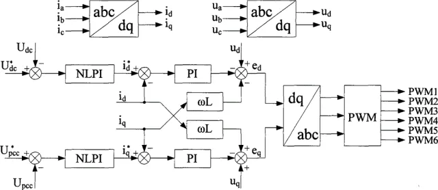
High switching speeds in SiC MOSFETs and Schottky diodes generate significant di/dt and dv/dt, making parasitic inductance and capacitance critical concerns. PCB designers must minimize commutation loop inductance through:
- Symmetrical, compact layouts with wide, short power traces or dedicated power planes.
- Kelvin connections for gate drive signals to separate high-current paths from sensitive control circuitry.
- Controlled-impedance routing and proper decoupling capacitor placement to suppress ringing and EMI.
Thermal management is equally important. SiC devices dissipate substantial heat even at high efficiency. Recommended PCB strategies include 3–10 oz copper layers, dense thermal via fields under device pads, and direct-bonded copper (DBC) or insulated metal substrate (IMS) integrations where extreme power density is required. High-Tg laminates and optimized stack-ups prevent delamination and maintain mechanical stability during thermal cycling.
Signal integrity and EMI/EMC compliance further require careful grounding schemes, shielding considerations, and creepage/clearance distances suited to high-voltage operation. Star grounding and separation of power and analog sections help maintain precision in gate drivers and control circuits.
Packaging Technologies and Their Impact on PCB Integration
SiC device packaging has evolved rapidly to support higher power density and reliability. Traditional aluminum wire bonding is giving way to copper wire bonding and silver sintering for chip-to-substrate and substrate-to-heatsink attachments. Silver sintering provides superior electrical and thermal conductivity, reduces thermal resistance by up to three times compared with solder, and extends module lifetime significantly.
Substrate materials are shifting from standard alumina DBC to silicon nitride, aluminum nitride, and active metal brazed (AMB) thick-copper substrates. These offer better thermal performance and mechanical strength, directly influencing the choice of PCB-level heat spreading and attachment methods.
Molded modules are increasingly preferred over potting for lower stray inductance and higher reliability. On the aluminum PCB, this trend favors designs with low-inductance bus bars, optimized via stitching, and compatible surface finishes that ensure reliable soldering or sintering interfaces during assembly.
Manufacturing Challenges and PCB Fabrication Implications
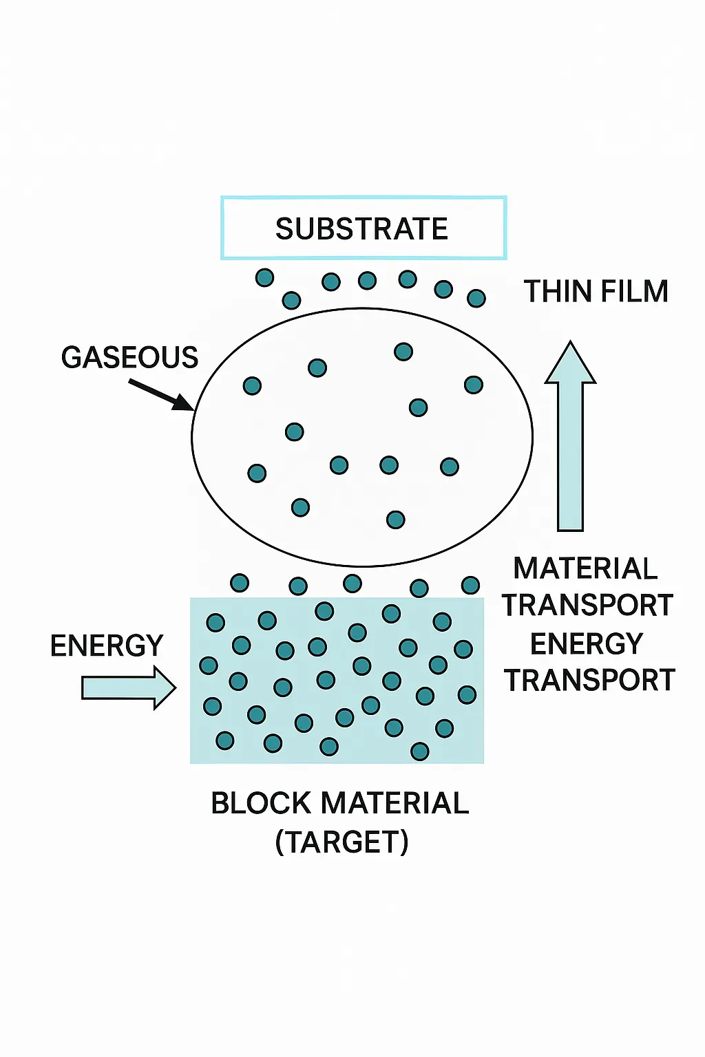
Producing high-quality SiC substrates and epitaxial layers involves precise control of crystal growth (primarily physical vapor transport), slicing, polishing, and epitaxy—processes that affect device cost and availability.
For PCB manufacturers, the key implications lie in supporting the resulting high-performance modules:
- Heavy copper and thick-copper PCBs for high-current paths.
- Advanced thermal management features such as embedded copper coins, metal-core PCBs, or hybrid constructions.
- Strict process controls for via filling, plating, and lamination to handle elevated operating temperatures and thermal expansion mismatches.
- High-reliability testing including thermal cycling, power cycling, and insulation resistance verification.
Challenges such as crystal defects, slow growth rates, and wafer yield directly influence device pricing and supply, prompting PCB designers to select proven, automotive-grade or industrial-grade SiC modules that balance performance with manufacturability.
Trends in SiC Module Packaging Evolution and Future PCB Optimization
Ongoing trends include double-sided silver sintering, nano-silver processes that lower bonding temperatures, and the adoption of AMB substrates for automotive and high-reliability applications. Molded packages with reduced inductance are becoming mainstream. These developments push PCB technology toward:
- Higher copper weights and finer feature sizes for power integrity.
- Integration of advanced thermal interface materials and embedded cooling solutions.
- Design-for-manufacturability practices that accommodate higher switching frequencies while maintaining yield in volume production.
As SiC adoption accelerates—driven primarily by new-energy vehicles and renewable energy—the demand for specialized PCBs capable of hosting these devices continues to grow. Aivon's advanced PCB manufacturing capabilities, including heavy copper, high-Tg materials, precise via structures, and thermal management solutions, enable engineers to realize the full potential of SiC in next-generation power electronics across automotive, industrial, telecom, and energy sectors.
Conclusion
Silicon carbide devices deliver transformative performance gains in power electronics, but their full potential is realized only through meticulous PCB design and manufacturing practices. By addressing high-speed layout, advanced thermal management, optimized packaging integration, and robust fabrication processes from the outset, engineers can achieve higher efficiency, greater power density, and superior reliability. As SiC adoption expands across electric vehicles, renewable energy, and industrial systems, specialized PCB solutions remain the critical enabler for scalable, high-performance power conversion.