Introduction
Resistors, capacitors, and inductors are the most common passive elements in circuits. Even when these components are not intentionally used, parasitic resistance, capacitance, and inductance are present throughout a design. Capacitors are more common than inductors in circuits, and some specialized analog ICs require capacitors for isolation.
Common On-Chip Capacitor Types
MOS capacitor: Uses parasitic Cgd, Cgb, and Cgs in the MOS structure, with gate and source/drain/body acting as electrodes and the oxide layer as the dielectric.
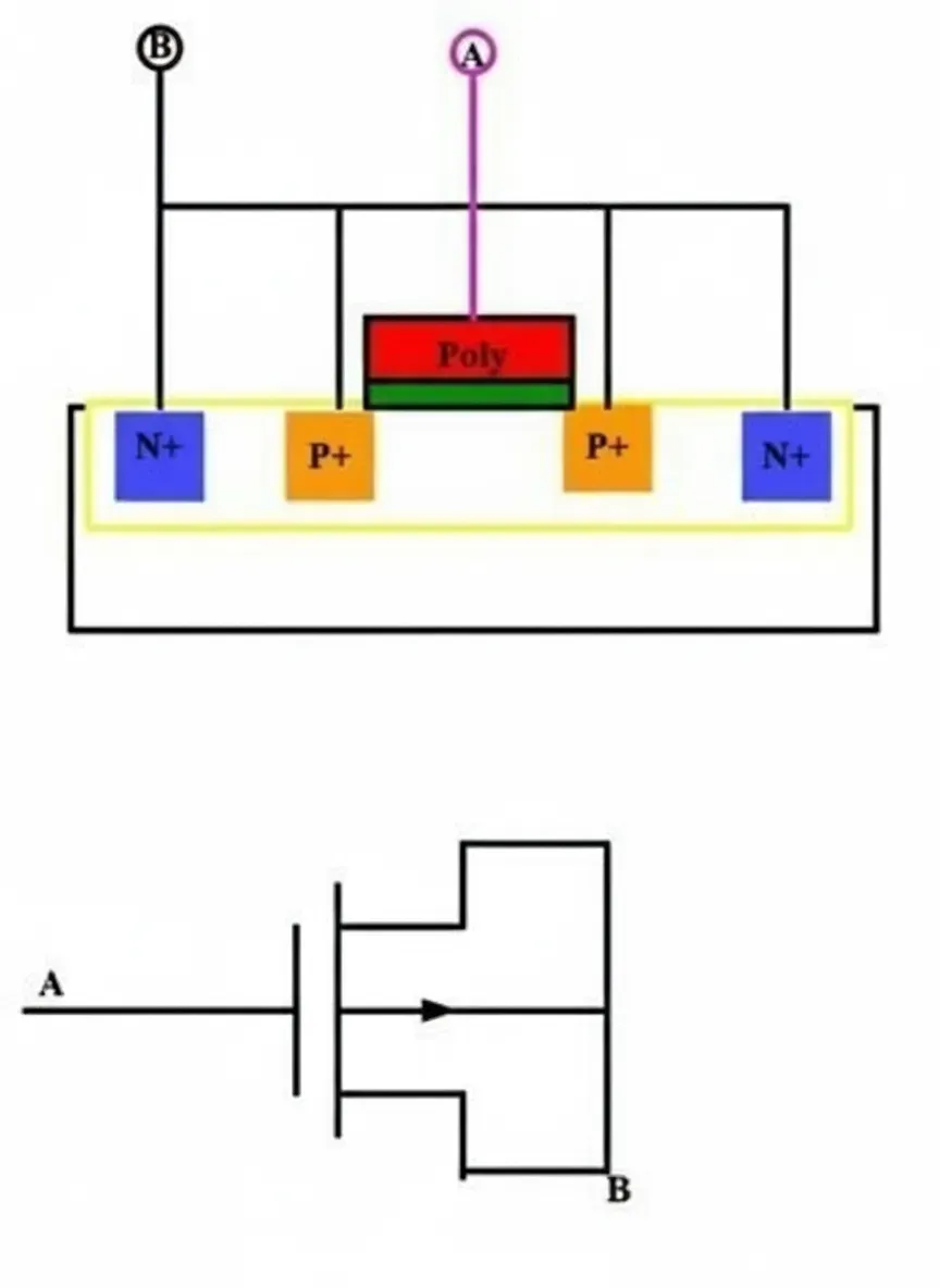
Figure 1. MOS capacitor schematic.
MOM capacitor: Metal-oxide-metal interdigitated capacitor that uses edge capacitance between metal lines on the same layer. In foundry processes, the gaps between same-layer metals are filled with SiCN for advanced (nanometer) processes or SiO2 for older (submicron) processes; this filler acts as the dielectric. As an interdigitated structure, MOM capacitors provide large capacitance and good symmetry.
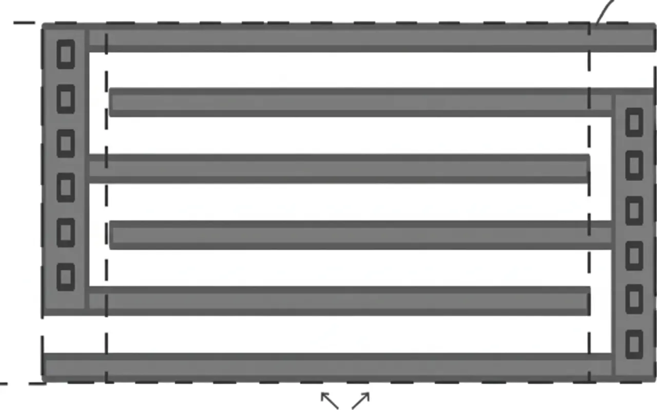
Figure 2. MOM capacitor schematic.
MIM capacitor: Metal-insulator-metal plate capacitor formed by two metal plates separated by an insulating layer. During fabrication, the inter-metal gaps are filled with an insulating material (SiCOH for nanometer processes or SiO2 for submicron processes). The two metal layers act as the plates and the inter-metal dielectric acts as the insulator. MIM capacitors provide accurate capacitance values, but as process nodes scale down and inter-metal dielectrics thin, MIMs become less suitable for advanced nodes. When using MIM capacitors, be aware of plasma charging damage: the antenna effect of the capacitor plates can cause damage, and fabs typically provide design rules to avoid such issues.
Capacitors and ESD
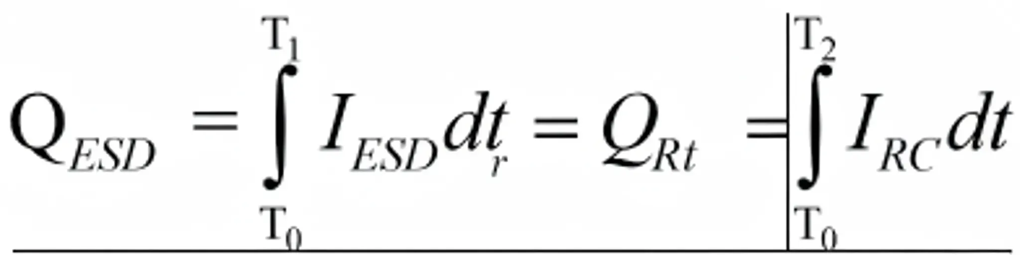
If considering only the capacitor itself for ESD performance, the requirement is simply that the voltage across it remains below its breakdown voltage. However, in some circuits, RC networks formed by capacitors and resistors influence the ESD behavior of the entire system. This effect has been encountered in practical work. The HBM waveform generator circuit and its waveform have been discussed in earlier material.
The HBM waveform uses the inherent response characteristics of an RC circuit, but the parasitic capacitances and inductances present in the HBM generator can cause deviations from the standard response waveform (the decay phase of the HBM waveform follows an exponential). In ESD testing, capacitors in a circuit usually fall into three categories relative to the ESD discharge path.
Capacitor Positions Relative to the ESD Discharge Path
Type 1 capacitor (in Figure 3): This capacitor is not connected to the ESD discharge path and is effectively open-circuit with respect to ESD. In this case, the capacitor has no effect on the circuit's ESD performance and is not affected by ESD.
Type 2 capacitor: This capacitor is in parallel with the ESD discharge path and does not negatively affect the ESD discharge. In the figure, X7R and AFE are two ESD protection devices with different parasitic capacitances. X7R exhibits lower capacitive reactance, while AFE has higher reactance. Observations show that protection devices with lower reactance allow larger ESD current peaks at the IC input and generally provide worse protection. Conversely, protection devices with higher reactance produce lower peak currents and smoother ESD pulses. Therefore, placing a capacitor in parallel with the protection device in the ESD discharge path increases the effective reactance, lowering the ESD pulse peak and making the waveform smoother. This spreads the energy and can improve ESD protection.
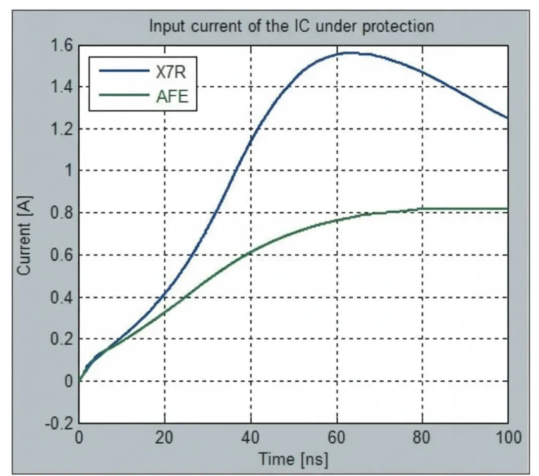
Figure 3. Effect of capacitors with different impedances on ESD waveform.
Series Capacitor Effects
Most critical is Type 3, which is less common. In port-to-port ESD discharge paths, a series capacitor may exist in the path, and the path can include parasitic resistances or other impedances R1 and R2. Experimental results indicate that the RC network formed by R1, R2, and C3 affects ESD performance. Testing excluded C3 failure due to voltage breakdown. With limited prior research on this configuration, the following is a reasoned hypothesis.
Overall, a series capacitor has the opposite effect of a parallel capacitor: series capacitance reduces the total capacitance in the discharge path, which narrows the ESD waveform and concentrates energy, making failures more likely. From the perspective of the ESD generator, a capacitor in series along the discharge path behaves like an impulsive source. By charge conservation, the total charge generated by the ESD source and the total charge that leaves the system are conserved (neglecting carriers generated by device avalanche, which are relatively small).
Charge redistribution alters the impulse current. R1, C3, and R3 can shorten the overall waveform duration T2, producing a higher transient impulse current. In effect, this RC network reshapes the ESD waveform and can degrade the ESD robustness of the circuit.
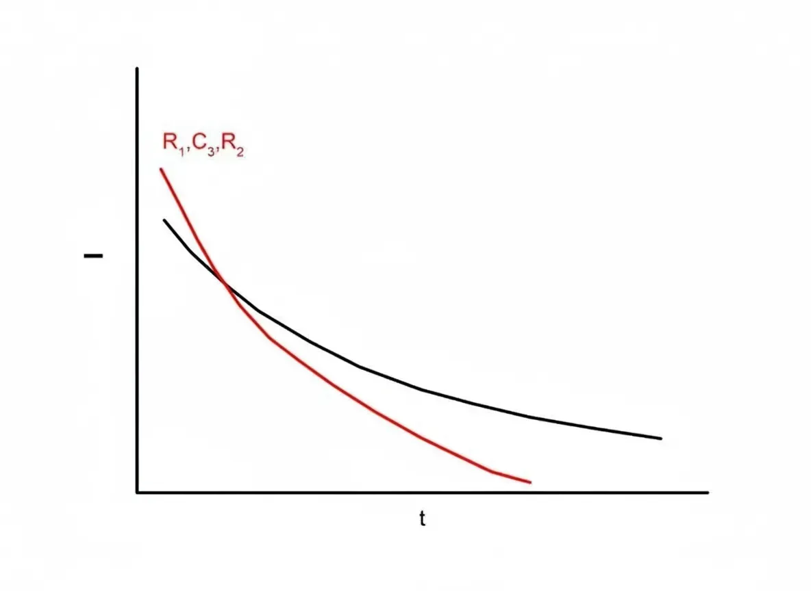
Figure 5. Waveform shaping effect of R1, C3, and R3 on ESD current.
Design Considerations
To improve ESD robustness, both GGNMOS and diodes should be paralleled as much as possible: this increases the capability to handle large currents and increases parasitic capacitance, which smooths the ESD current and disperses energy. However, added parasitic capacitance is unacceptable for high-speed circuits. Therefore, ESD designers must coordinate with circuit designers to balance protection and signal integrity.