Overview of Silicon Nitride Films in Microelectronics and MEMS
Silicon nitride (SiN or Si3N4) thin films are indispensable in microelectromechanical systems (MEMS), semiconductor processing, and precision electronics. They serve as structural layers, etch masks, passivation layers, and insulators due to their excellent chemical resistance, mechanical strength, electrical insulation properties, and thermal stability.
Low-stress silicon nitride films are particularly valuable for applications requiring thicker films or freestanding structures, where high intrinsic stress can cause cracking, warping, or delamination. Low-Pressure Chemical Vapor Deposition (LPCVD) is a preferred method for achieving controlled, low-stress SiN films with superior uniformity and quality.
Key Applications of Low-Stress Silicon Nitride
MEMS Devices: Silicon nitride functions as a structural material in accelerometers, gyroscopes, pressure sensors, and flow sensors. Its hydrophobicity, high elastic modulus (~250 GPa), low thermal conductivity (~20 W/(m.K)), and excellent dielectric properties (resistivity ~10^14 Ohm.cm, bandgap ~5 eV) make it ideal for passivation and insulation in harsh environments.
TEM Windows and Advanced Imaging: Low-stress SiN membranes (typically 20-200 nm thick, near-zero stress) replace traditional copper grids in transmission electron microscopy (TEM). They offer superior strength, chemical inertness, and high-temperature stability for in-situ heating, liquid-cell, or sensitive sample analysis.
Broader Electronics Relevance: In semiconductor and sensor manufacturing, SiN layers support diffusion barriers, anti-reflective coatings, and protective films. For high-reliability applications like automotive, aerospace, and industrial sensors, low-stress films enhance mechanical stability and long-term performance.
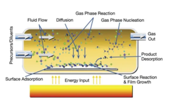
What is LPCVD and Why It Excels for Silicon Nitride
Low-Pressure Chemical Vapor Deposition (LPCVD) operates at reduced pressures (typically 10-1000 Pa or 200-500 mTorr), contrasting with atmospheric pressure CVD. Lower pressure improves gas diffusion, resulting in excellent step coverage, uniformity, and film density across large wafer batches.
For stoichiometric Si3N4, LPCVD uses dichlorosilane (SiH2Cl2, DCS) and ammonia (NH3) at 700-900 degrees Celsius. Standard processes yield high-tensile-stress films (>1 GPa), limiting thickness before failure. Low-stress films are achieved by depositing silicon-rich silicon nitride through adjusted gas ratios.
Achieving Low-Stress LPCVD Silicon Nitride Films
Increasing the DCS/NH3 ratio introduces excess silicon, reducing tensile stress. Optimal conditions for near-zero stress include a DCS/NH3 ratio around 6:1, temperature of ~850 degrees Celsius, and pressure of 500 mTorr. This silicon-rich composition allows thicker, crack-free films suitable for MEMS membranes and structural elements.
Process Steps (Typical Horizontal or Vertical Furnace):
- Introduce reactant gases (DCS, NH3) with controlled flow rates and inert carrier gas (e.g., N2) into the reaction chamber.
- Gases flow toward heated substrates.
- Adsorption of reactants on the wafer surface.
- Surface migration and chemical reactions form the SiN film.
- Byproducts are evacuated, maintaining low pressure.
Film properties are highly tunable via temperature, pressure, gas ratios, and deposition time.
Process and Equipment Considerations for Uniformity and Quality
Temperature Uniformity
Variations up to 20 degrees Celsius across a furnace tube can cause significant stress gradients. Optimizing temperature zones (e.g., elevating center temperature) can reduce wafer-to-wafer stress variation to less than 3%.
Gas Flow and Depletion
Reactant concentration decreases downstream, leading to thickness non-uniformity. Higher gas flow rates and optimized wafer boat designs mitigate this.
Vertical vs. Horizontal LPCVD Systems
Vertical furnaces offer superior performance with double-tube chambers for better gas uniformity, reduced particle contamination, lower oxygen levels (minimizing native oxide), and wafer rotation for enhanced across-wafer consistency. These advantages translate to higher yield and reproducibility, critical for volume manufacturing of MEMS and sensor components.
Relevance to PCB Manufacturing and Electronics Integration
While LPCVD is a front-end semiconductor/MEMS process, low-stress SiN films play supporting roles in advanced PCB and electronics assembly:
- Sensor Integration: MEMS sensors using SiN structures are assembled onto PCBs in industrial control, automotive, and medical devices. Reliable, low-stress films ensure sensor accuracy and durability.
- Semiconductor Packaging: SiN layers in wafers or interposers benefit HDI PCBs and advanced packaging.
- Manufacturing Synergies: Expertise in thin-film deposition processes informs broader materials engineering and reliability testing for complex electronics assemblies, including thermal management and mechanical stability under stress.
High-reliability PCB manufacturers work closely with semiconductor processes to support customers developing integrated sensor systems and power electronics.
Industry Trends
Demand for low-stress SiN continues to grow with MEMS expansion in IoT, autonomous systems, and medical diagnostics. Advances in LPCVD equipment and process control enable larger wafers, tighter specifications, and integration with other thin films for multifunctional structures.
FAQ
Q1: What causes high stress in standard LPCVD SiN films, and how is it reduced?
A1: Stoichiometric films have high tensile stress (>1 GPa). Silicon-rich films (higher DCS/NH3 ratio) significantly lower stress, enabling thicker, stable membranes.
Q2: What are typical thicknesses for low-stress SiN in TEM windows?
A2: 20 nm to 200 nm with near-zero stress for optimal mechanical stability and electron transparency.
Q3: Why choose vertical LPCVD systems?
A3: They provide better uniformity, lower contamination, and improved process control compared to horizontal systems, enhancing yield for precision applications.