Feedback topologies form the foundation of stable, high-performance analog circuits on printed circuit boards. Engineers must identify whether feedback is positive or negative, series or shunt at the input and output ports, because these choices directly determine input/output impedance, gain stability, bandwidth, and noise performance. In PCB implementation, the physical layout, trace routing, via placement, and component selection must support the intended feedback behavior while minimizing parasitic inductance, capacitance, and thermal effects.
Identifying Feedback Type on the PCB
A systematic procedure helps classify feedback without ambiguity:
- Determine polarity by breaking the loop and observing signal inversion. Opposite polarity indicates negative feedback, which stabilizes gain and reduces distortion.
- Short the input source to test series versus shunt behavior at the input. If the feedback path still influences the input node, the topology is series (high input impedance).
- Short the output load to test series versus shunt behavior at the output. Persistent influence indicates series feedback at the output (high output impedance).
These tests translate directly to PCB layout decisions. Series feedback at the input often requires careful routing of high-impedance nodes to avoid stray capacitance from adjacent traces or ground planes. Shunt configurations benefit from low-inductance return paths and proper via stitching.
Four Feedback Topologies and Their PCB Implications
Negative feedback topologies map to the four ideal amplifier types:
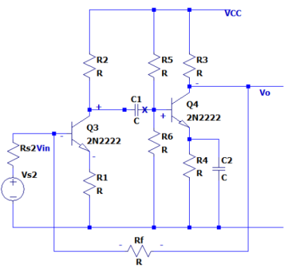
- Voltage-series (series-shunt): High input impedance, low output impedance — ideal voltage amplifier. On the PCB, place the feedback resistor network close to the op-amp inputs and outputs to minimize loop area and inductive pickup. Use controlled-impedance traces where high-frequency signals are present.
- Current-series (series-series): High input and high output impedance — transconductance amplifier. Source degeneration resistors and current-sensing elements must be routed with Kelvin connections on the PCB to eliminate voltage drops from trace resistance.
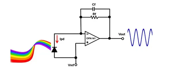
- Voltage-shunt (shunt-shunt): Low input and low output impedance — transimpedance amplifier. Common in photodiode or current-to-voltage conversion circuits. Low-impedance nodes require wide traces or copper pours and careful grounding to prevent ground bounce.
- Current-shunt (shunt-series): Low input impedance, high output impedance — current amplifier. Guard traces or driven shields around sensitive nodes help maintain the low input impedance on the board.
Positive feedback, created by reversing the feedback connection point, finds use in Schmitt triggers and oscillators but demands tight layout control to prevent unintended oscillations from parasitic paths.
Buffer Amplifiers in Feedback Systems
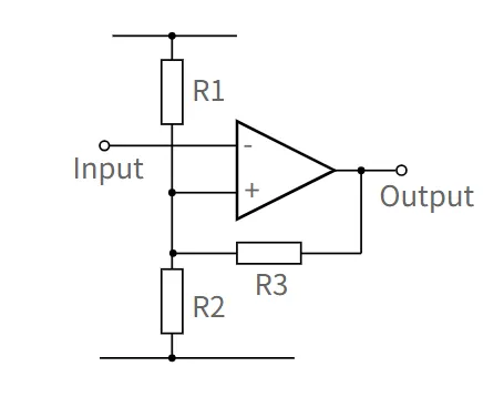
Buffer amplifiers isolate stages and provide impedance transformation, a critical function when cascading analog blocks on a PCB. A voltage buffer (unity-gain configuration) presents very high input impedance and very low output impedance, preventing loading effects between a high-impedance sensor and a subsequent low-impedance stage.
In op-amp implementations, the noninverting input receives the signal while the output feeds back directly to the inverting input.
On the PCB this requires:
- Short, direct feedback traces to preserve phase margin.
- Proper decoupling capacitors placed immediately adjacent to power pins.
- Ground plane cuts or star grounding to avoid common-impedance coupling.
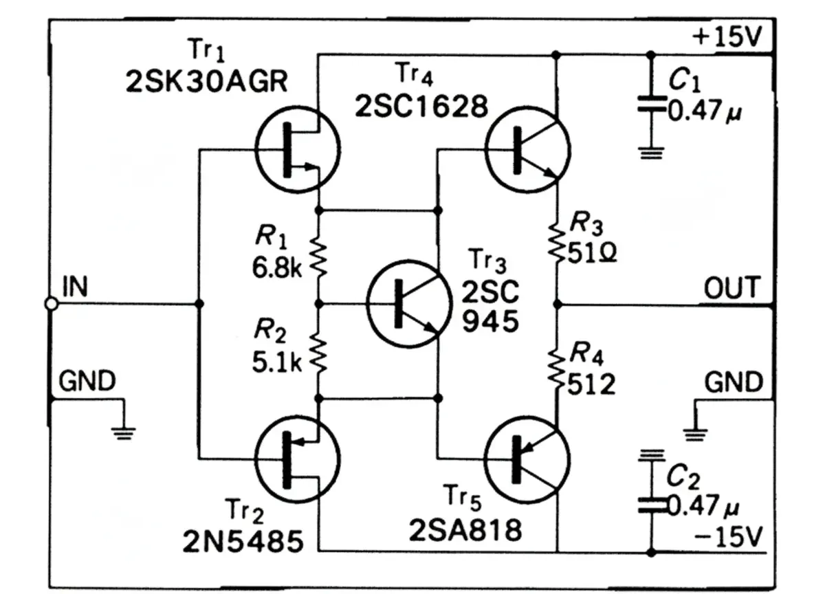
Current buffers perform the complementary function, presenting low input impedance and high output impedance. Push-pull complementary FET buffers extend this capability to higher speeds and power levels. Matched N-channel and P-channel devices in a complementary pair deliver fast rise/fall times and low output impedance while maintaining high input impedance. When embedded inside an op-amp feedback loop, device mismatch offsets become negligible.
PCB considerations for push-pull buffers include:
- Thermal management — output transistors may require copper pours or heatsinks connected through thermal vias.
- Matching of FET characteristics to minimize DC offset.
- Selection of devices with appropriate ft and low output capacitance.
- Increased bias current for linear-region operation at high frequencies.
Component Selection and Manufacturing Constraints
Feedback resistors and capacitors directly influence stability, bandwidth, and noise. Choose low-temperature-coefficient resistors and low-ESR capacitors. On multilayer PCBs, consider dielectric constant and loss tangent of the substrate material when signals exceed a few hundred megahertz. Thicker copper layers improve current handling and thermal dissipation in power stages.
HDI techniques or controlled-impedance stack-ups become necessary for high-speed feedback loops. Via stitching around sensitive nodes reduces inductance. Proper solder-mask and surface-finish choices affect high-frequency performance and long-term reliability.
Practical Design Practices for Reliable PCB Implementation
- Keep feedback loop area small to reduce parasitic inductance and radiated EMI.
- Separate analog and digital ground domains with single-point connections when both exist on the same board.
- Place bypass capacitors as close as possible to IC power pins; use multiple values in parallel for broadband decoupling.
- Account for thermal gradients — place heat-generating components away from precision feedback networks.
- Simulate layout parasitics early; tools that extract trace inductance and capacitance help predict stability margins before fabrication.
Conclusion
Effective feedback circuit design and buffer amplifier implementation ultimately depend on the seamless integration of circuit theory with PCB manufacturing realities. By rigorously applying topology analysis, optimizing layout for minimal parasitics, selecting appropriate materials and components, and addressing thermal and EMI constraints during the fabrication process, engineers achieve superior signal integrity, long-term reliability, and consistent production yields. These practices are essential across demanding sectors such as automotive electronics, industrial control systems, telecommunications infrastructure, and precision instrumentation. Partnering with an experienced PCB manufacturer ensures that design intent is preserved through every stage of fabrication, from stack-up definition to final assembly and testing.