What Is a Chip IO Circuit?
IO (Input/Output) circuits form the interface between a chip's internal core logic and the external world. Located at the die periphery, these circuits handle critical functions such as:
- Level Shifting: Converting between internal core voltages and external signal levels.
- Drive Strength: Providing sufficient current to drive capacitive loads and multiple fan-outs while maintaining acceptable rise/fall times.
- ESD Protection: Safeguarding against electrostatic discharge events that could damage the chip.
Robust IO design is essential for reliable communication with other chips, sensors, memory, and peripherals on the PCB.
IO Circuit Classifications
Input IOs
Input IOs are relatively straightforward, often implemented as buffers (e.g., inverters). Variants include those with or without weak pull-up/pull-down resistors to establish default states when undriven.
Output IOs
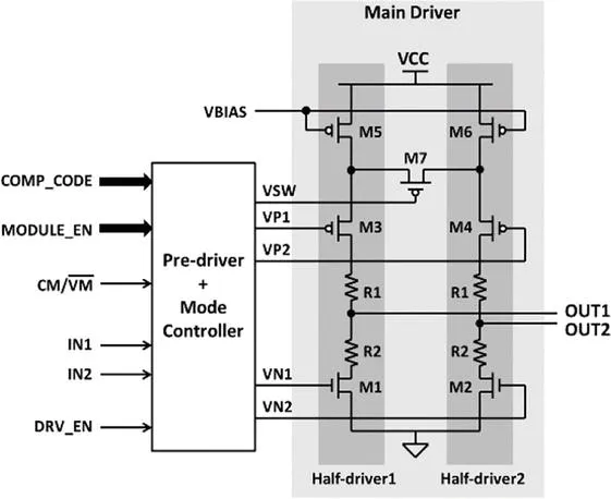
- Push-Pull (Totem-Pole): Standard inverter-like structure capable of actively driving both high and low levels.
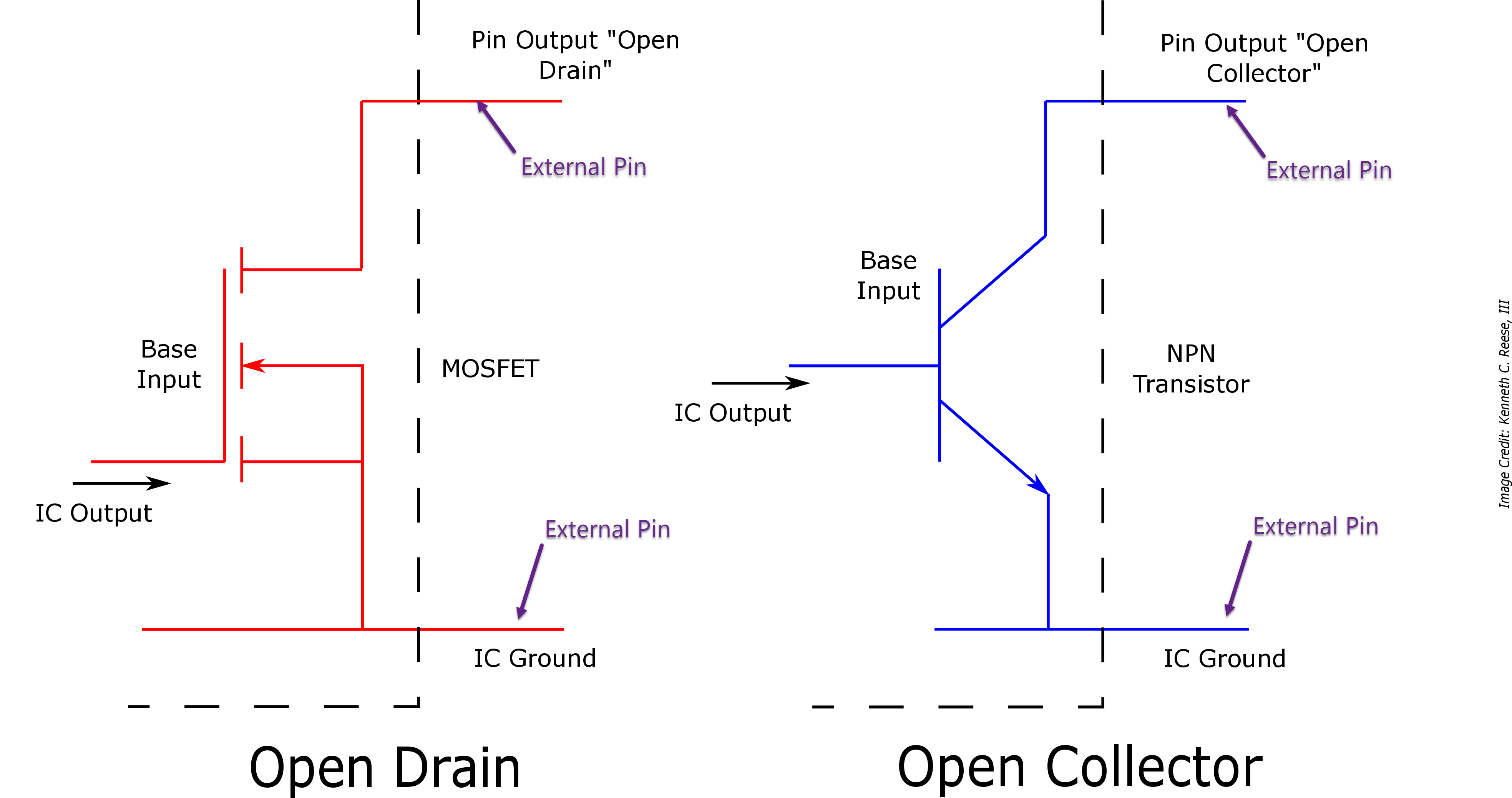
- Open-Collector/Open-Drain (OC/OD): Requires an external pull-up resistor. Advantages include flexible level shifting, wired-AND functionality, but introduces rise-time dependency on the pull-up value.
- Tri-State Outputs: Add a high-impedance (Z) state in addition to logic 0 and 1. Enables bus sharing where multiple devices connect to the same lines; only one driver is active at a time via output enable (OE) control. Unidirectional and bidirectional variants exist.
Key Challenges in IO Circuit Design
While basic principles are well-established, real-world performance is heavily influenced by ground bounce - a dynamic shift in the chip's internal ground potential relative to the PCB ground due to package parasitic inductance.
When multiple outputs switch simultaneously, rapid current changes (di/dt) across bond wire/package inductance create voltage spikes on the internal ground. This can shift input thresholds, causing false logic levels or intermittent behavior, particularly under CMOS VIH/VIL specifications.
Effective IO design must guarantee reliable VIH (input high voltage) and VIL (input low voltage) margins even under worst-case ground bounce conditions across process, voltage, and temperature (PVT) corners.
Measuring VIH/VIL Under Ground Bounce Conditions
Two primary simulation methods help characterize input thresholds under dynamic conditions:
Ramp Input Method
Apply a slow linear ramp to the input. Record the voltage at first incorrect switching (VIL) and last incorrect switching (VIH). Use a shallow slope (e.g., 10 mV over two switching periods) for accuracy.
Step Input Method
Apply discrete voltage steps. Identify thresholds from steps immediately before/after incorrect transitions. This method is often preferred for PVT sweeps as it allows focusing computation on critical edge regions, reducing simulation time while maintaining accuracy.
Both approaches yield consistent results when properly parameterized.
PCB and System-Level Implications
IO circuit performance directly affects board design:
- Signal Integrity: Drive strength, slew rate control, and impedance matching must align with PCB trace characteristics.
- Power/Ground Distribution: Multiple ground pins, decoupling, and low-inductance paths minimize bounce.
- ESD and Protection: Board-level considerations complement on-chip protection.
- Mixed-Signal Integration: Careful placement and routing prevent noise coupling in systems combining digital, analog, and high-speed IO.
Advanced PCB manufacturing - controlled impedance, HDI, and high-reliability processes - helps realize the full potential of sophisticated IO designs in applications like automotive, industrial, telecommunications, and computing.
FAQ
Q1: What is ground bounce and why is it critical for IO design?
A1: Ground bounce is the inductive voltage spike on internal ground during simultaneous switching. It can shift input thresholds and cause functional errors if not properly managed.
Q2: When are tri-state outputs typically used?
A2: In shared bus architectures where multiple devices connect to the same lines and only one should drive at any time.
Q3: How do OC/OD outputs differ from push-pull?
A3: OC/OD cannot actively drive high and rely on external pull-ups, offering flexibility in level shifting and wired logic but slower rising edges.