Overview
NIO introduced the NX9031 autonomous driving chip alongside the ET9 on December 23, 2023, and announced that the ET9 will enter production in 2025 with this chip. Public information released so far highlights a 5 nm process, more than 50 billion transistors, LPDDR5X memory, a 32-core CPU in a big.LITTLE configuration, a high-dynamic-range ISP with 26-bit internal width, 6.5 Gpixel/s pixel processing capability, and ASIL-D functional safety support.
Foundry and Process
In the current IP-centered semiconductor era, many required IP blocks can be procured if budget allows, so NIO producing a 5 nm SoC is not inherently surprising. Only TSMC and Samsung provide 5 nm foundry services; Samsung is a likely candidate for NX9031 manufacturing because TSMC foundry costs are typically higher and TSMC's automotive 5 nm capacity is heavily booked by customers such as Qualcomm. Samsung has fewer 5 nm automotive customers, so its capacity may be more available.
Ranking SoCs for Autonomous Driving
Evaluating autonomous driving SoCs cannot be based solely on AI throughput. Memory bandwidth is as important as AI compute, and CPU performance is critical. Autonomous driving software stacks are complex and consume substantial CPU resources. The stack includes middleware such as SOME/IP, Adaptive AUTOSAR, DDS, ROS, and base software like custom Linux BSPs, OS abstraction layers, virtual machines, memory management, drivers, and communication protocols. Application-layer workloads such as path planning, high-definition mapping, and behavior decision also heavily load CPUs. CPUs additionally manage task scheduling, memory movement, and coordination of AI execution. In this context, CPU performance is a central factor, with AI accelerators serving as specialized coprocessors for tasks like feature extraction, classification, BEV transforms, vector map mapping, or occupancy estimation.
Suggested weighting for SoC ranking: AI compute, memory bandwidth, CPU compute, GPU compute, then process node. Memory bandwidth and AI compute should be weighted equally. GPUs can be complementary; many automotive AI workloads use INT8, while GPUs can handle FP32 when beneficial. Published AI throughput numbers can be inconsistent, so the most reliable indicator is MAC array size. For example, Google TPU v1 had 65,000 FP16 MACs at 0.7 GHz, giving 65000*0.7G*2 = 91 TOPS. Tesla's first FSD used two NPUs with 9,216 INT8 MACs each at 2 GHz, yielding 2*2*2G*9216 = 73.7 TOPS. Smaller process nodes generally imply lower power for equivalent performance.
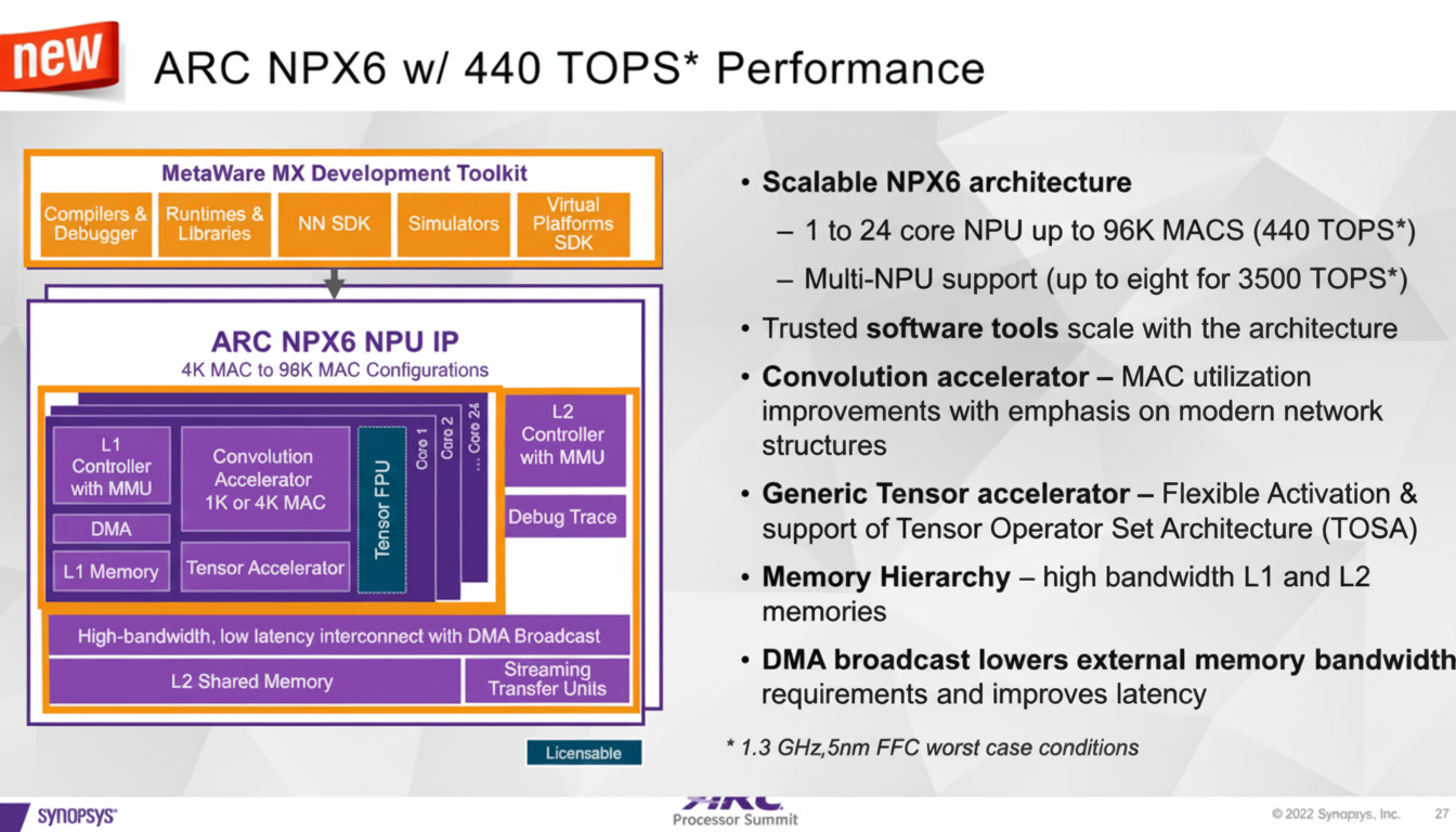
IP Examples and Multi-Chip Scaling
Synopsys offers an IP supporting up to eight NPUs with a total of 3,500 TOPS. A single NPU in that IP can include up to 96,000 MACs at 1.3 GHz, giving 2*1.3G*96000 = 249.6 TOPS in dense mode. With sparse modes such as EDSR, effective throughput can increase by about 76% to roughly 440 TOPS.
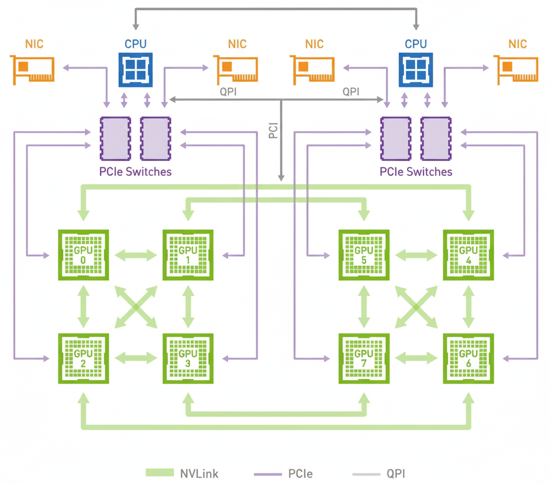
NX9031 has not published peak AI throughput. Some commentary has suggested NX9031 replaces four NVIDIA Orin units and thus delivers 4 * 254 = 1,008 TOPS. That assumption is flawed. If four Orins are connected via Ethernet switches, effective aggregate compute scales far less than 4x due to interconnect limits; realistic aggregate throughput might only increase by about 20%, yielding roughly 300 TOPS for four units. Achieving a true 4x increase requires an interconnect with NVLink-like bandwidth, which typical Ethernet switches cannot provide.
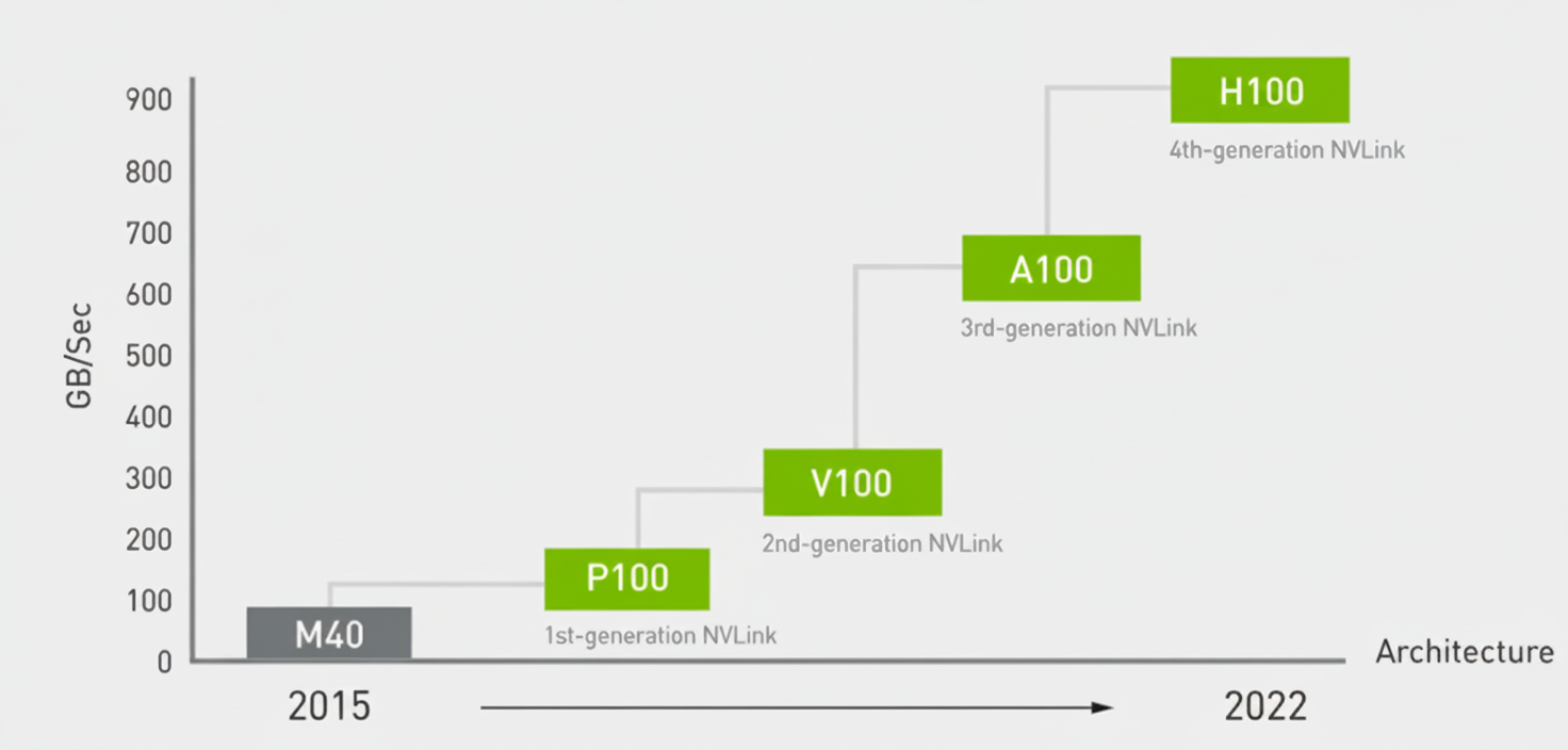
NVIDIA DGX systems illustrate chip-level interconnect scaling. GPUs require a CPU host and use high-bandwidth NVLink between GPUs and PCIe between CPU and GPUs. Fourth-generation NVLink bandwidth reaches 900 GB/s. By contrast, high-end production Ethernet switch port bandwidth is orders of magnitude lower, so Ethernet-based clustering cannot match NVLink scaling without specialized routing silicon such as Broadcom Qumran3D, which offers extremely high upstream bandwidth but at high cost and still subject to endpoint limitations.
Memory and Bandwidth
NIO specifically calls out LPDDR5X, but it did not disclose the memory bus width, so memory bandwidth is unknown. LPDDR5X supports up to 8,533 MT/s. Most automotive and embedded SoCs today use LPDDR4 or LPDDR5; LPDDR5X became standardized in 2021, with products appearing around 2020. Higher-bandwidth alternatives used in some deployments include GDDR6 and HBM.
Estimating a bus width of 128 to 256 bits for NX9031 suggests memory bandwidth in the range of approximately 136 to 273 GB/s. Increasing memory bus width raises die area and cost because the memory controller and PHY scale with width; this is why many vendors prefer larger caches rather than much wider external memory interfaces.
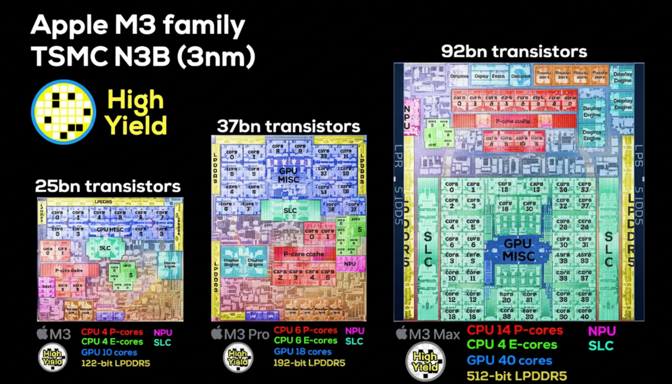
For comparison, Apple M3 chips demonstrate memory-controller die area growth with width: M3 uses a 128-bit interface, M3 Pro 192-bit, and M3 Max 512-bit. The M3 Max memory controller occupies substantially more die area than M3 and M3 Pro, illustrating how width increases drive die size and cost.
ISP and Image Processing
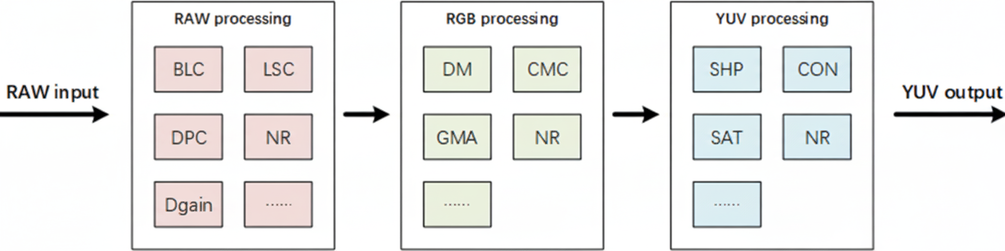
NX9031 emphasizes a high-performance image signal processor. Historically, some systems used discrete ISP chips, but modern SoCs generally integrate ISPs to reduce latency as pixel counts and AI usage increase. Typical ISP pipelines perform black level correction, defective pixel correction, digital gain, lens shading correction, demosaicing, color matrix correction, gamma correction, and then operate in the YUV domain for sharpening, contrast, and color saturation, with denoising stages inserted throughout the pipeline.
Synopsys IP example data referenced above.
NVIDIA Orin's internal ISP handles 1.85 Gpixel/s. NX9031 advertises 6.5 Gpixel/s, roughly three times Orin. In the mobile sector, some ISPs reach even higher rates. For example, MediaTek Dimensity 9000's ISP reaches 9 Gpixel/s, while Qualcomm implementations are typically somewhat lower. Higher pixel/s capacity allows support for higher-resolution sensors or multiple sensors; approximately 1.3 Gpixel/s can support a 100 MP sensor with compression, and uncompressed 100 MP can require around 3.2 Gpixel/s. NX9031's 6.5 Gpixel/s could support sensors in the 200 MP range with compression strategies.
NX9031 specifies a 26-bit internal ISP width versus typical mobile ISP widths around 18 bits. Most image sensors output 10- or 12-bit ADC data. ADC dynamic range determines sensor bit depth; for example, Sony IMX490 at 10-bit ADC achieves 40 fps, while at 12-bit ADC the frame rate is 30 fps. A wider ISP internal width can enable higher effective throughput and dynamic range handling.
CPU and Functional Safety
NIO highlights CPU capability at 615k DMIPS. For reference, NVIDIA Orin reports about 228k DMIPS using 12 Cortex-A78AE cores, with L2 and L3 caches of about 3 MB and 6 MB respectively and core frequencies around 2.0-2.2 GHz, implying roughly 19k DMIPS per core in that configuration. Given a 5 nm node, NIO could run cores at higher frequencies and/or increase cache sizes, making per-core DMIPS higher. A plausible NX9031 design might use around 20 big cores producing up to 24k DMIPS each plus 12 small Cortex-A55 cores, which would align with the stated aggregate of 615k DMIPS.
For ASIL-D functional safety, SoC designs commonly add an MCU island with lockstep cores, often using two to four Cortex-R52 cores in lockstep. This approach is used in several automotive-focused SoCs such as Qualcomm SA8255 and SA8755.
Concluding Notes
Publicly available details on NX9031 show an ambitious SoC with competitive process technology and a focus on memory, ISP, CPU performance, and functional safety. Key unknowns remain, notably the memory interface width and the exact architecture and MAC array size of the AI accelerators, which are crucial to fully assess system-level performance for automotive workloads.