Introduction
In a previous article titled "NVIDIA ADAS - NVIDIA DriveOS Introduction" the software stack was described. This article focuses on NVIDIA's commercially deployed hardware for automated driving, the Orin SoC.
Orin has seen strong demand. Several automakers and autonomous driving companies are developing on the Orin platform, including SAIC, IM Motors, Li Auto L9, NIO ET7, XPeng new P7, WM Motor M7, BYD, Volvo XC90, Plus.ai, Cruise, Zoox, Didi, Pony.ai, AutoX, Momonta, and others. The platform is positioned as a high-performance compute SoC for automotive applications.
1. NVIDIA Automotive SoC Evolution
Since 2015 NVIDIA has entered the automotive SoC and vehicle compute platform domain to provide compute capability for automated driving. NVIDIA has released automotive-grade SoCs roughly every two years while steadily increasing compute performance. The Xavier SoC delivered around 30 TOPS in 2020. Orin, released for commercial use, delivers up to 254 TOPS. At the 2022 fall GTC NVIDIA announced Thor, with stated performance claims far beyond previous generations.
1.1 Xavier platform
NVIDIA introduced the Xavier platform at CES 2018 as an evolution of Driver PX2. Xavier was positioned as a high-performance SoC for autonomous driving, capable of processing sensor data from cameras, radar, lidar, and ultrasound with improved power efficiency and reduced size. Jetson AGX Xavier established a reference point for compute density and AI inference at the edge.
The XPeng P7, launched in April 2020, was among the first production vehicles to deploy the NVIDIA DRIVE AGX Xavier platform. The P7 configuration included multiple cameras, millimeter-wave radars, ultrasonics, and an open NVIDIA DRIVE OS.
Xavier is manufactured on TSMC 12 nm FinFET process, integrating approximately 9 billion transistors on a 350 mm2 die. The CPU is an NVIDIA-custom 8-core ARM 64 architecture (Carmel). Xavier integrates a Volta GPU (512 CUDA cores) with support for FP32/FP16/INT8. At 20 W power the single-precision FP performance is about 1.3 TFLOPS, with Tensor core performance around 20 TOPS, scalable up when configured for higher power.
Xavier is a highly heterogeneous SoC integrating up to eight different processor or hardware acceleration blocks, enabling real-time concurrent execution of many algorithms for sensor processing, localization and mapping, perception, and planning.
Beyond compute, Xavier exposes rich I/O resources suitable for automotive integrations.
Xavier's primary processor can be used as part of an ASIL-B capable functional safety solution. Some automotive central compute reference designs pair Xavier SoC with an Infineon TC297 MCU to provide an overall architecture suited for L3/L4 automated driving: the Xavier SoC handles perception, fusion, and planning while the TC297 MCU addresses ISO 26262 functional safety requirements (ASIL-C/D) as a safety core for supervisory monitoring, redundancy management, gateway communications, and vehicle control.
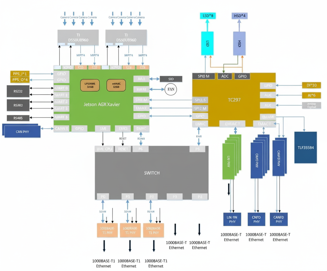
The dual Xavier plus TC297 MCU block diagram follows the same domain separation approach used in many vehicle architectures: driving domain (NVIDIA), vehicle control domain (MCU), and a separate cockpit domain typically based on mature Android smartphone technology. While convergence to a central architecture is possible, many production vehicles still adopt a three-domain architecture.
1.2 Orin platform
NVIDIA announced Orin in December 2019 as its next-generation SoC and compute platform for automated driving and robotics. Orin integrates ARM Hercules CPU cores and NVIDIA's next-generation GPU architecture. The Orin SoC contains about 17 billion transistors, roughly twice Xavier, and integrates 12 ARM Hercules cores with an Ampere-based GPU delivering significantly higher performance; the SoC targets up to 200 TOPS (INT8) and entered volume production with automotive customers in 2022.
At GTC 2020 NVIDIA described the DRIVE AGX Orin platform, which can host two Orin SoCs and two Ampere GPUs to scale compute from entry-level ADAS to robotaxi L5 systems, with platform performance up to 2000 TOPS. Orin is aimed at concurrent execution of multiple automated driving applications and deep neural network models.
Orin is designed to meet ISO 26262 ASIL-D functional safety requirements for automotive use cases. Leveraging an advanced 7 nm process, Orin offers high compute while maintaining energy-efficient operation; for example, 200 TOPS with a TDP around 50 W.
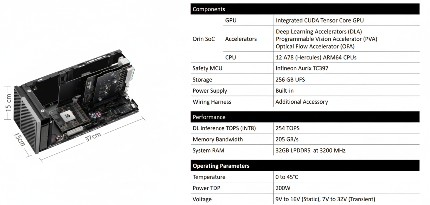
Key Jetson AGX Orin SoC performance characteristics are summarized in vendor materials and product briefs.
1.3 Thor platform
NVIDIA DRIVE Thor is described as a next-generation centralized vehicle compute platform capable of running advanced driver assistance and in-vehicle infotainment on a single safety-certified system. DRIVE Thor was announced with very high compute figures and a planned production timeline starting around 2025. The platform intends to consolidate driving and cockpit domains into fewer compute domains by using multi-domain isolation and safety techniques, enabling a vehicle to run multiple operating systems concurrently (for example Linux, QNX, and Android) while isolating time-critical processes.
Thor includes new CPU and GPU innovations and a Transformer engine in GPU Tensor cores to improve deep neural network accuracy and enable efficient temporal processing of video as single perception frames.
Reference: NVIDIA DRIVE Thor blog
2. Orin Architecture Overview
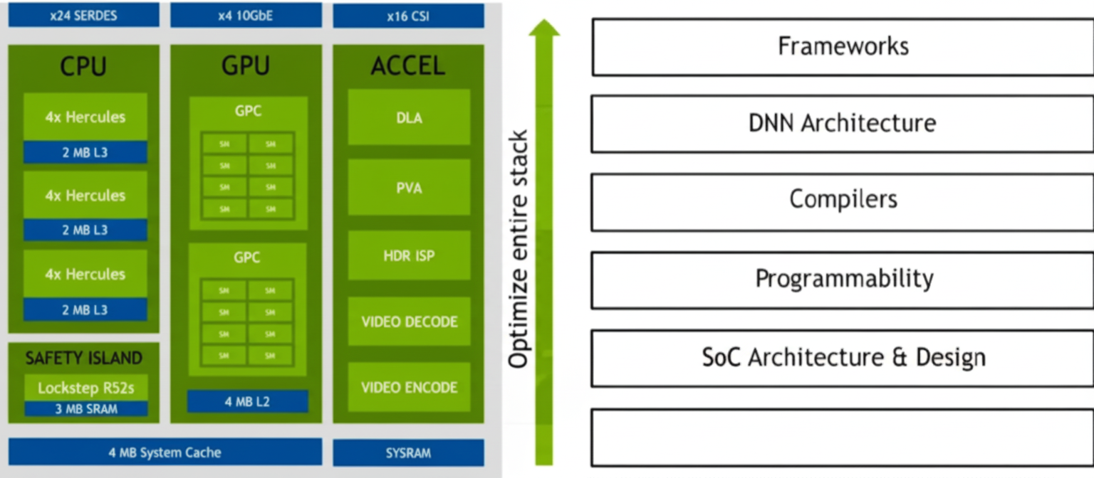
Using Orin-X as an example, the CPU complex includes an Arm Cortex-A78AE-based main CPU cluster for general high-performance compute, and an Arm Cortex-R52-based Functional Safety Island (FSI) that provides isolated on-chip compute resources to reduce dependence on external ASIL-D safety CPUs.
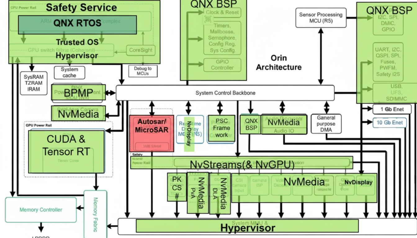
The GPU is an NVIDIA Ampere GPU that provides parallel compute for CUDA and supports tools such as TensorRT for low-latency, high-throughput deep learning inference. Domain-specific hardware accelerators (DSAs) offload various compute tasks from main compute engines to improve throughput and energy efficiency.
The internal architecture is organized into functional blocks: low-level OS BSPs, real-time RTOS components, multimedia processing modules (sensor processing MCU R5, PVA, DLA, audio processor), classic AUTOSAR modules for the safety island lock-step R52s, security services, and neural network processing modules (CUDA and TensorRT).
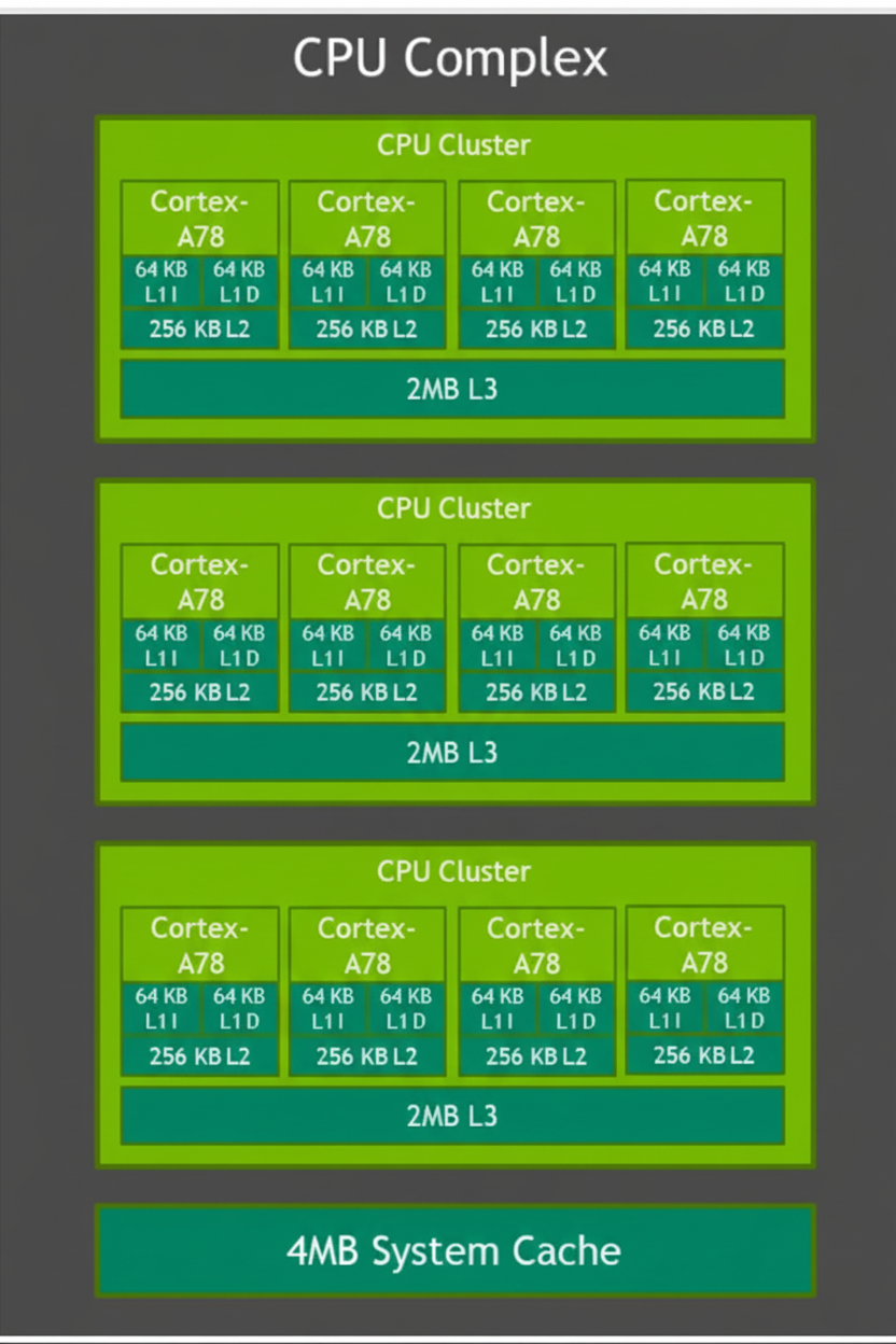
2.1 CPU
Orin replaces the previous custom Carmel CPU with ARM Cortex-A78 cores manufactured on a 5 nm process for general high-speed computing. Orin-X includes 12 Cortex-A78 cores and a Cortex-R52-based Functional Safety Island to provide isolated on-chip resources for ASIL-D level functional safety without requiring an additional external ASIL-D CPU.
The CPU complex supports debugging, power management, interrupt controllers, error detection and reporting, and performance monitoring via PMUv3 units in each core. These units collect statistics during runtime across processor and memory subsystems.
2.2 GPU
Orin uses an Ampere GPU composed of Graphics Processing Clusters (GPCs). Each GPC contains multiple Texture Processing Clusters (TPCs), and each TPC contains streaming multiprocessors (SMs). Each SM holds L1 cache and contributes to the overall L2 cache. In Orin the GPU totals 2048 CUDA cores and 64 Tensor cores. NVIDIA reports INT8 sparse throughput of 170 TOPS (Tensor cores), dense INT8 throughput of 54 TOPS, and FP32 throughput around 5.3 TFLOPS from CUDA cores.
Ampere GPUs support advanced parallel processing, CUDA development, Tensor Core acceleration, and graphics features such as real-time ray tracing. Key GPU features include structured sparsity doubling throughput, increased floating-point throughput per cycle, enhanced L1 cache bandwidth and shared memory, and improved asynchronous compute and L2 cache compression.
2.3 Accelerators
Domain-specific hardware accelerators (DSAs) such as DLA and PVA are dedicated engines to accelerate vision and deep learning workloads with high throughput and low power. The vision accelerator PVA is a vector-processing DSP optimized for computer vision, ADAS, and perception pipelines. PVA clusters contain vector processing units with instruction caches and vector data stores, designed to execute vision kernels efficiently with low latency.
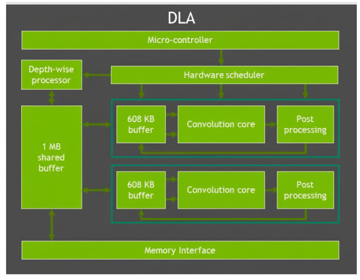
DLA is a fixed-function engine to accelerate neural network inference layers such as convolutions, activations, pooling, normalization, and fully connected layers. DLA supports optimized structured sparsity and has a hardware scheduler to maximize utilization. Note: some lower-power Orin variants may omit DLA.
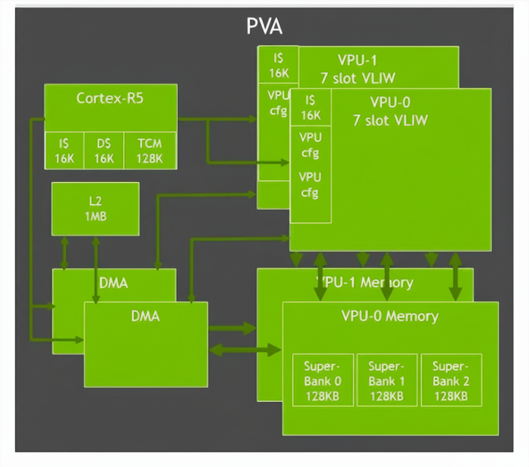
2.4 Second-generation vision accelerator: PVA and VIC
PVA in Orin is upgraded to dual 7-way VLIW vector processing units with dual DMA and Cortex-R5 control, supporting vision operations such as filtering, transforms, image pyramids, feature detection, and FFT. Orin also includes a Gen 4.2 Video Imaging Compositor (VIC) 2D engine for lens distortion correction, temporal denoise, sharpening, and pixel processing tasks like color space conversion, scaling, blending, and composition.
NVIDIA provides a Vision Programming Interface (VPI) software library to orchestrate hardware units (PVA, VIC, CPU, GPU, encoders). VPI includes image processing and classical computer vision algorithms such as box filters, convolutions, rescaling, remapping, Harris corner detection, KLT feature tracking, optical flow, and background subtraction.
2.5 Memory and communication
The following diagram shows how Orin components communicate via the on-chip memory fabric and DRAM.
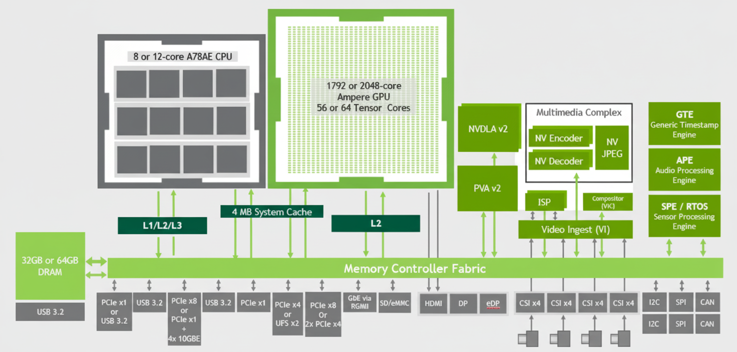
Orin supports up to 64 GB LPDDR5 in a 256-bit configuration and up to 64 GB eMMC storage. DRAM can operate at up to 3200 MHz with per-pin signaling, delivering up to 204.8 GB/s memory bandwidth, which is higher than previous-generation solutions.
3. Automated Driving Platform Architecture Based on Orin
Typical SoC system architectures for vehicles include an SoC plus one or more MCUs, or sometimes a three-chip approach. Because SoCs offer superior compute, they are favored for front-end perception and planning workloads, while MCUs are used for high-assurance control tasks due to their higher functional safety levels.
There is ongoing debate whether an SoC alone can replace separate high-assurance MCUs in vehicle control. NVIDIA SoCs provide ample AI and CPU compute for L2+ and higher automated driving systems, but vehicle control requires proven functional safety and large production volume deployments to validate replacements for traditional vehicle MCUs.
3.1 Safety considerations
Orin includes Cortex-R52 cores to implement a Functional Safety Island that can achieve ASIL-D capability. For complete vehicle control domains, a separate supervisory MCU (SMCU) is commonly included to implement vehicle control and fail-safe behaviors. Typical choices for such MCUs include Infineon AURIX family or Renesas RH850 family. In NVIDIA development platforms an SMCU such as TC397 can often be found providing power control and fault-handling coordination with the SoC.
Secure boot and chained boot flows are used to ensure integrity of low-level boot stages. Bootloaders and U-Boot images can be signed and verified, with keys stored in one-time programmable fuses. Redundant boot paths are supported for fault tolerance.
3.2 Functional Safety Island (FSI)
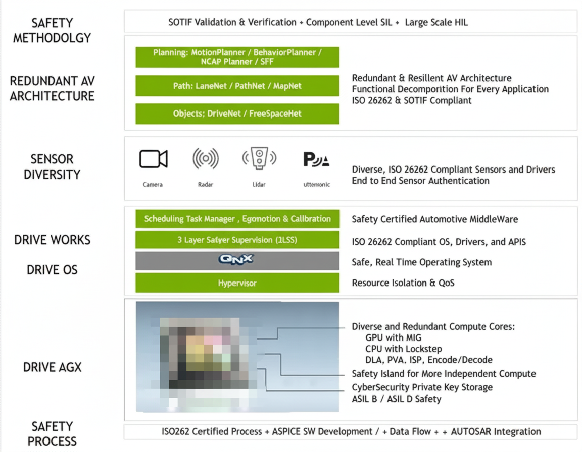
The figure below illustrates how FSI and related low-level drivers and boot components are integrated into NVIDIA SoCs. Orin targets ASIL-D capability through ASIL decomposition across SoC hardware and per-core safety mechanisms, combined with ASIL-D development processes applied to safety flows, Drive AGX platform, Drive OS, DriveWorks, sensor interfaces, redundancy, and safety policies.
The FSI contains Cortex-R52 and Cortex-R5F clusters with dedicated I/O controllers, independent voltage rails, oscillators and PLLs, and on-chip SRAM to minimize interactions with other SoC modules. Cortex-R52 implements safety-critical lock-step CPU configurations (DLS) and can run classic AUTOSAR RTOS workloads. Cortex-R5F acts as a Cryptographic Hardware Security Module (CHSM) for secure CAN-based use cases and secure onboard communications (SecOC).
FSI features include tightly coupled memory per safety core, 5 MB of on-chip RAM in the island for code and data, dedicated I/Os for external communications, hardware safety mechanisms such as CRC/ECC/parity/timeouts, and logical isolation to provide sufficient error recovery time between islands and the rest of the SoC.
3.3 Tegra Security Controller (TSEC)
Tegra Security Controller is an on-chip information security subsystem with a trusted root ROM, IMEM/DMEM, crypto accelerators (AES, SHA, RNG, PKA), key management, and secure storage. TSEC provides an on-chip Trusted Execution Environment (TEE) for trusted code and is used for tasks such as secure video playback and protected link management.
Key TSEC capabilities include HDCP management for HDMI outputs, platform security control services to protect assets (keys, fuses, features), key management and protection, attestation services for secure boot and runtime authentication, and security monitoring to detect physical or software attacks and apply mitigation strategies.
3.4 Security Engine (SE)
The Security Engine provides hardware acceleration for cryptographic algorithms and key protection. TZ-SE access is restricted to trusted software regions; NS/TZ-SE can be configured for access by non-secure software as needed. SE supports NIST-compliant symmetric and asymmetric cryptography, side-channel countermeasures, hardware key access controls, key wrapping/unwrapping, key derivation, RNG-based key generation, and hardware key isolation for AES key slots.
4. GPU Programming with CUDA
CUDA is the unified compute architecture used to program NVIDIA GPUs. It sits between the application and device drivers and provides developer libraries, a runtime environment, and a driver interface. CUDA and GPU acceleration are central to training and inference workloads for deep learning and machine learning used in automated driving.
4.1 GPU software architecture
AI algorithms for automated driving are often highly parallel. Deep neural networks for perception and machine learning for inference and decision tasks benefit from massive parallelism on GPUs. GPUs efficiently execute many independent computations in parallel, which matches the data-parallel nature of convolutional and other neural network operations. A single convolution may be slower on a GPU compared with a CPU, but the GPU's parallel execution across thousands of threads yields far greater throughput for complete workloads.
NVIDIA supplies a software stack including CUDA libraries (cuBLAS, cuFFT, cuSolver, Thrust), communication libraries (NCCL, NVSHMEM), and specialized inference runtimes (TensorRT), which together support AI development across workstations, servers, and cloud environments. CUDA is specific to NVIDIA GPUs and organizes programs into host (CPU) and device (GPU) code. The device code, or kernel, runs on the GPU, and data is transferred between host memory and GPU memory. PCI Express bandwidth is a potential bottleneck; avoiding frequent host-device transfers improves efficiency.
4.2 CUDA programming model
In CUDA, programmers structure kernels to exploit thousands of concurrent threads and use on-chip shared memory to reduce DRAM bandwidth requirements. Optimized CUDA libraries and the runtime environment reduce development effort and provide abstractions for memory management, device access, and execution scheduling. For large-scale parallel problems, CUDA effectively hides memory latency and leverages GPU execution units to handle thousands of threads concurrently. When workloads are not parallelizable at scale, CUDA may not provide expected performance benefits.
Conclusion
Understanding SoC architecture is valuable for software engineers designing automotive solutions. Software architects should map software requirements to available hardware paths, confirm performance suitability, and identify hardware modules that can accelerate functionality. For driver development, enumerate required hardware modules and define driver APIs that encapsulate services for higher-level software.
This article summarizes Orin based on vendor materials and a range of public references. Detailed device datasheets and field application engineering support are available from the vendor under registration and specific support agreements; those resources were not reproduced here.