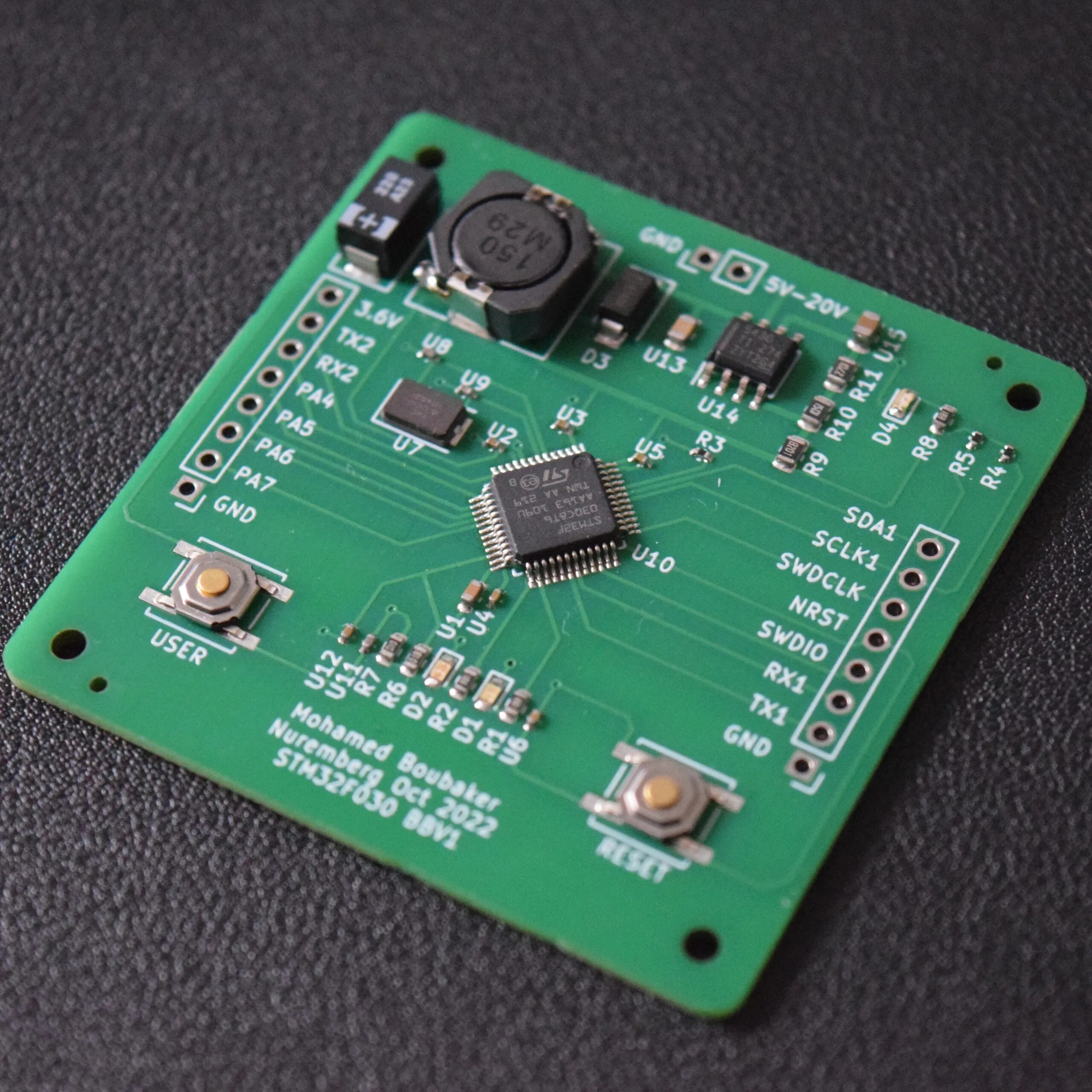
What Are Double-Sided PCBs and Through-Hole Components?
Double-sided printed circuit boards (PCBs) represent a significant advancement over single-layer designs, featuring conductive pathways on both their top and bottom surfaces. This dual-layer architecture dramatically increases routing flexibility and component density, making them indispensable in today's compact and sophisticated electronic devices, from consumer gadgets to intricate industrial systems.
Through-hole components are electronic parts characterized by their leads, which physically pass through pre-drilled holes in the PCB. These leads are then soldered to corresponding pads, often on the opposite side of the board, establishing both a secure mechanical anchor and a reliable electrical connection. Common examples include various resistors, capacitors, and connectors. Unlike their surface-mount counterparts, through-hole components are valued for their superior mechanical strength and ease of manual manipulation, especially critical when components are populated on both sides of a double-sided board.
Why Does Soldering on Double-Sided Boards Require Special Attention?
Soldering components onto double-sided PCBs presents distinct challenges compared to single-layer boards. The presence of conductive traces and components on both surfaces necessitates a careful approach to avoid unintended consequences. One primary concern is thermal management; excessive heat applied to one side can inadvertently damage sensitive components or cause delicate traces to lift on the opposing side. Furthermore, through-hole components in a double-sided context often demand soldering on both layers to guarantee a robust connection, particularly in applications involving higher currents where joint integrity is paramount.
Another significant hurdle is preventing solder bridges or accidental short circuits between closely spaced pads and traces across the board. Achieving precision and employing the correct soldering technique are key to mitigating these issues. The subsequent sections will delve into specific soldering methods designed to address these complexities effectively in double-sided PCB assembly.
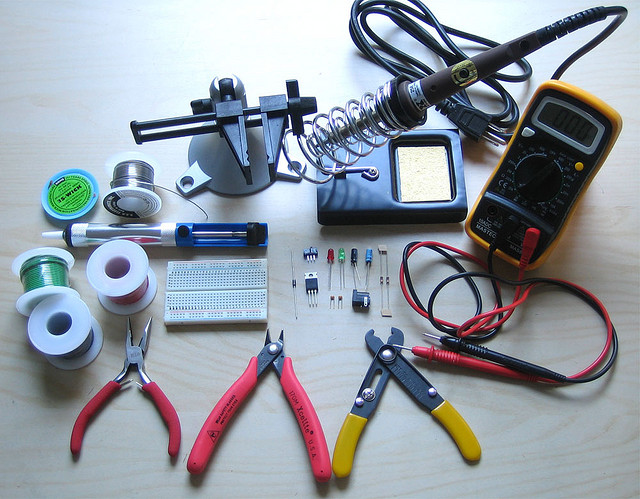
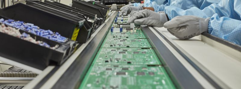
What Essential Tools and Materials Are Needed for Double-Sided PCB Soldering?
Before embarking on any soldering task involving through-hole components on double-sided PCBs, assembling the correct set of tools and materials is crucial for ensuring a smooth and successful process.
Core Soldering Equipment
● Temperature-Controlled Soldering Iron: A station with precise temperature control and a fine tip (1mm or smaller) is ideal for intricate work, typically set between 300°C and 350°C.
● Solder Materials:
○ Solder Paste: Essential for reflow soldering, this combines solder alloy and flux for precise application on pads.
○ Solder Wire: For manual soldering, choose a lead-free or leaded wire with a diameter of 0.5mm to 1mm.
● Flux: This material is vital for cleaning metal surfaces and improving solder flow, which helps prevent cold solder joints.
Support and Correction Tools
● Desoldering Tools: A solder wick or a desoldering pump is indispensable for correcting errors or removing excess solder efficiently.
● PCB Holder: A stable holder is highly recommended to secure the board, allowing you to work on both sides without slippage.
● Cleaning Supplies: Isopropyl alcohol and a small brush are necessary for removing flux residues post-soldering, ensuring a clean finish.
Specialized Production Equipment
● Reflow Oven or Hot Air Gun: These are critical for reflow soldering processes, especially when using solder paste with through-hole components.
● Wave Soldering Equipment: For large-scale production, this specialized machinery handles bulk soldering of through-hole components.
How to Prepare a Double-Sided PCB for Through-Hole Component Assembly?
Thorough preparation is a cornerstone of successful soldering. These steps ensure your double-sided PCB is optimally ready for through-hole component placement and soldering:
Initial Board Inspection and Cleaning
● Inspect for Flaws: Begin by closely examining the PCB for any manufacturing imperfections, such as misaligned drilled holes or damaged traces. Verify that all through-holes are clear of obstructions and debris.
● Clean the Surfaces: Use isopropyl alcohol and a suitable brush to meticulously remove any dust, grease, or oxidation that may have accumulated on the pads and in the holes. A clean surface is paramount for optimal solder adhesion.
Component Insertion and Securing
● Orient and Insert Components: Carefully place each through-hole component into its designated holes, ensuring the leads pass through to the opposite side. For double-sided boards, pay close attention to the specific side each component is intended for according to the design documentation.
● Secure Components: To prevent components from shifting during soldering, slightly bend their leads on the opposite side of the board. Alternatively, employ a PCB holder or adhesive tape to firmly hold parts in position.
What Soldering Techniques Are Best for Double-Sided Through-Hole PCBs?
Achieving robust solder joints on double-sided PCBs with through-hole components can be accomplished using several key methods, each suited to different production volumes and project intricacies.
1. Manual Soldering with Solder Paste and Hot Air
This hybrid technique bridges traditional manual soldering with modern paste application, making it suitable for PCB prototype manufacturing or small batch runs, especially in mixed-technology assemblies.
● Application: Precisely apply a small amount of solder paste to the pads surrounding the through-holes on both sides of the PCB, using a syringe or a small stencil for control.
● Component Placement: Insert the through-hole components, ensuring their leads penetrate the paste-covered pads.
● Reflow: Use a hot air gun or a small reflow oven to evenly heat the board. This melts the solder paste, forming the electrical and mechanical joints. Lead-free solder pastes typically reflow between 220°C and 250°C.
● Inspection and Rework: Visually inspect all joints for proper wetting and fillet formation. If necessary, use a soldering iron and wire solder to manually touch up any incomplete joints.
2. Through-Hole Reflow (THR) Soldering
Through-Hole Reflow (THR) is an adaptation of the standard reflow process, primarily for surface-mount devices, now applied to through-hole components on double-sided PCBs to streamline assembly in automated environments.
● Design Considerations: The PCB design must feature appropriately sized pads and stencil apertures, often with an overprint of 0.2mm to 0.3mm beyond the pad size, to ensure sufficient solder paste volume around the through-holes.
● Paste Application: Apply solder paste to the pads on one side of the PCB using a stencil.
● Component Insertion: Insert through-hole components so their leads protrude to the opposite side.
● Reflow Profile: Process the PCB through a reflow oven using a specific temperature profile. This typically involves preheating (150°C-180°C for 60-90 seconds), a soak phase, and a reflow peak (235°C-250°C for 20-40 seconds).
● Double-Sided Processing: For boards with components on both sides, a second reflow pass might be necessary, using a lower temperature profile to prevent remelting the previously soldered joints.
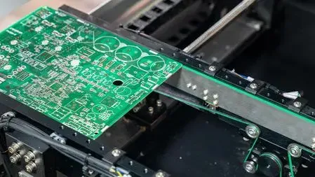
3. Wave Soldering
Wave soldering is a high-volume process ideal for soldering through-hole components, particularly on the bottom side of double-sided PCBs in mass production settings.
● Flux Application: Apply flux to the bottom side of the PCB to clean the metal surfaces and enhance solder flow.
● Preheating: Preheat the PCB to approximately 100°C-130°C. This activates the flux and minimizes thermal shock during contact with molten solder.
● Solder Wave Contact: Pass the PCB over a wave of molten solder (typically 250°C-260°C for lead-free alloys) at a controlled conveyor speed (e.g., 1-2 meters per minute). The wave makes contact with the through-hole leads and pads on the bottom surface, forming the solder joints.
● Component Protection: If the top side of the double-sided PCB also has components, they must be protected with heat-resistant masking or adhered with high-temperature glues to prevent dislodging. Alternatively, top-side components can be manually soldered after the wave soldering process.
● Cooling and Cleaning: Allow the PCB to cool gradually to prevent thermal stress, then thoroughly clean any remaining flux residue.
Key Tips for Achieving Excellent Solder Joints on Double-Sided PCBs
To consistently produce high-quality solder joints when working with through-hole components on double-sided PCBs, keep these practical guidelines in mind:
Process Optimization and Inspection
● Prevent Overheating: Limit the exposure time to soldering heat—whether from an iron or a reflow oven—to avoid damaging sensitive components or lifting PCB traces. For manual soldering, aim for contact times under 3-5 seconds per joint.
● Assess Joint Quality: After soldering, inspect each joint. Ideal solder joints are shiny, form a concave fillet around the lead, and show good wetting. Dull, cracked, or excessively rounded joints often indicate a "cold solder joint," which can lead to intermittent failures.
● Ensure Proper Ventilation: Soldering generates fumes, especially when using flux or leaded solder. Always work in a well-ventilated area, or use a fume extractor to protect your respiratory health.
Component Handling and Post-Soldering Verification
● Verify Component Orientation: Before making permanent connections, double-check the orientation of polarized components, such as diodes and electrolytic capacitors. Correcting errors on a double-sided board can be significantly more challenging than on a single-sided one.
● Conduct Post-Soldering Tests: After assembly, use a multimeter to perform continuity checks and test for any unintended shorts between adjacent pads or traces on both sides of the PCB. This helps confirm the integrity of your connections.
Common Pitfalls to Avoid in Double-Sided PCB Soldering
Even experienced assemblers can encounter challenges when soldering double-sided PCBs. Being aware of common mistakes can help you prevent them:
Solder Application and Thermal Management
● Insufficient Solder Volume: Applying too little solder is a frequent issue, leading to weak or unreliable joints. Ensure that enough solder paste or wire is used to form a complete and robust fillet around the through-hole lead.
● Solder Bridges: Excessive solder can create unintended electrical connections (solder bridges) between closely spaced pads. If this occurs, use a desoldering wick or pump to carefully remove the excess material.
● Thermal Damage: Prolonged application of heat can cause significant damage, such as delaminating pads or destroying components. Work efficiently, and consider using a heat sink on sensitive parts to dissipate heat quickly.
Design and Process Alignment
● Ignoring Design Limitations: Always ensure that your PCB design is compatible with your chosen soldering method. For example, specific pad spacing might be necessary for wave soldering, or precise stencil designs for effective through-hole reflow.
● Inadequate Cleaning: Failing to properly clean flux residues can lead to corrosion or electrical leakage over time, compromising board reliability.
Conclusion: Mastering Through-Hole Soldering on Double-Sided PCBs
Soldering through-hole components onto double-sided PCBs might initially appear complex, but with the correct techniques and a methodical approach, it becomes a highly manageable and rewarding task. Whether you opt for the precision of manual soldering with solder paste, the efficiency of reflow soldering, or the speed of wave soldering, each method offers distinct advantages tailored to various project demands. By diligently following the preparatory steps, applying the chosen soldering technique, and meticulously inspecting your work, you can consistently achieve robust, high-quality solder joints that are crucial for the performance and longevity of your electronic designs.
Always remember that proper preparation, selecting the most appropriate soldering method for your specific setup, and thorough post-soldering inspection are key. With consistent practice, you will develop the confidence and expertise needed to excel in double-sided PCB assembly, producing professional-grade results on every project.