What is PCB Silkscreen and Why Is It Important?
The Role of Silkscreen in Circuit Board Assembly
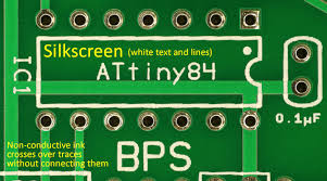
Printed Circuit Boards (PCBs) are foundational to modern electronics, with every element contributing to their function and assembly. The silkscreen layer, a non-conductive ink applied to the PCB surface, is one such crucial detail. This layer contains essential text and symbols like reference designators, polarity indicators, and assembly instructions, simplifying component identification and correct board assembly.
Impact of Font Size on Readability and Functionality
Selecting an appropriate silkscreen font size is crucial for ensuring these markings are readable during assembly, inspection, and repair. A font that is too small can lead to costly errors, while one that is excessively large may clutter the board and obstruct component placement. This guide delves into best practices for silkscreen font sizes, emphasizing component identification and clarity for PCB assembly.
Why Does Silkscreen Font Size Matter for Component Labels?
Preventing Assembly Errors and Streamlining Troubleshooting
The silkscreen layer acts as a visual guide for engineers, technicians, and assembly personnel. It clearly labels components with reference designators (e.g., "R1" for a resistor, "C3" for a capacitor), indicates polarity for crucial components like diodes and capacitors, and sometimes includes test points or version numbers. If the font size is inadequate, these markings become unreadable, causing mistakes during assembly or complicating troubleshooting efforts.
Imagine an assembler incorrectly placing a component because the tiny reference designator was illegible. Such inaccuracies can cause production delays or, worse, lead to product malfunctions. Conversely, overly large fonts can consume valuable board space, particularly in high-density designs, resulting in a cluttered and confusing layout. Achieving the right balance in font size ensures the silkscreen fulfills its purpose without compromising the PCB's overall design and functionality.
What Factors Influence Silkscreen Legibility on PCBs?
Several elements dictate how readable your silkscreen markings will be. Understanding these factors is key to choosing the correct font size and style for your PCB design.
Key Dimensions: Font Height and Stroke Width
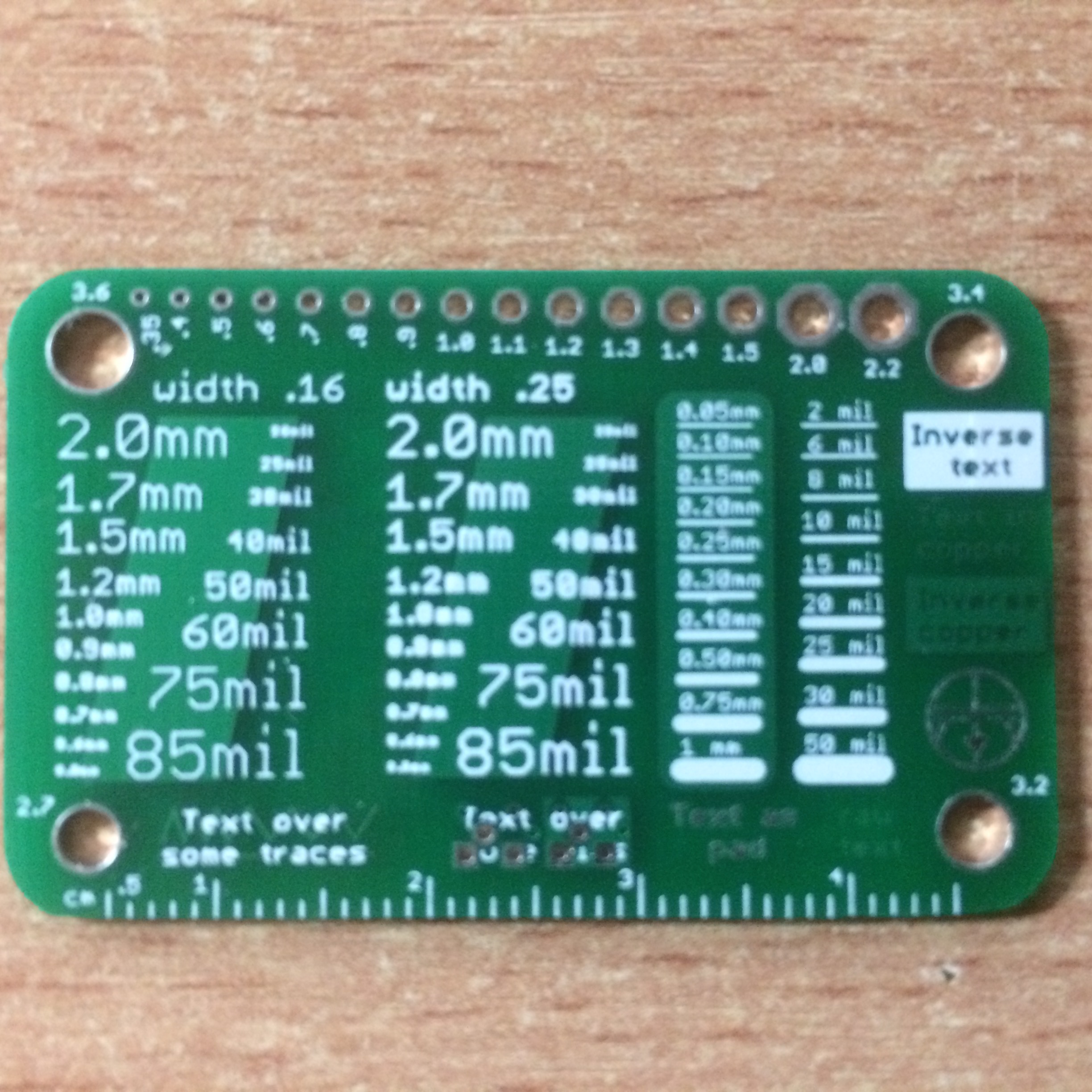
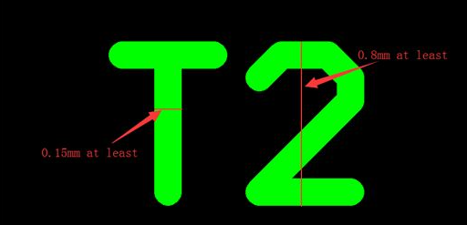
The most critical factors for legibility are the font's height and the thickness of its lines (stroke width). A font height of at least 0.040 inches (1.016 mm) is widely considered the minimum for readability under typical conditions. The stroke width should ideally be around 0.006 inches (0.152 mm) to ensure lines are distinct without merging.
Board Characteristics and Viewing Conditions
For compact or densely populated PCBs, space for silkscreen is limited, necessitating the minimum recommended font size. Larger boards with fewer components allow for slightly larger fonts (up to 0.060 inches or 1.524 mm) for improved visibility. Additionally, assembly and inspection often occur in varying lighting, so a size that is clear in a well-lit environment might be difficult to read in dimmer conditions. Accessibility for individuals with vision impairments also favors adhering to minimum recommended sizes.
Manufacturing Constraints
Not all PCB manufacturers can produce extremely fine silkscreen details. If the font size or stroke width is too small, markings may blur or become illegible during printing. Always consult your online pcb manufacturer regarding their silkscreen resolution capabilities, which typically range from 0.004 to 0.008 inches (0.102 to 0.203 mm) for stroke width.
What Are the Recommended Silkscreen Font Sizes for PCB Assembly?
Based on industry benchmarks and practical experience, here are the recommended font sizes for PCB silkscreen markings, specifically for component identification and reference designators.
● Minimum Font Height: 0.040 inches (40 mils or 1.016 mm)
● Minimum Stroke Width: 0.006 inches (6 mils or 0.152 mm)
● Ideal Font Height for High Visibility: 0.050 to 0.060 inches (1.27 to 1.524 mm)
● Maximum Font Height: Avoid exceeding 0.080 inches (2.032 mm) unless ample space is available, as larger fonts can clutter the board.
These dimensions are derived from PCB design standards and feedback from assembly professionals, ensuring reference designators and other markings remain clear throughout manual and automated assembly.
Preferred Font Styles for Readability
Beyond just size, the style of the font significantly affects its legibility. Simple, sans-serif fonts such as Arial or Helvetica are much easier to read at smaller sizes compared to serif or decorative fonts. It's best to avoid italicized or overly stylized text, as these can become distorted when printed onto a PCB surface.
Best Practices for Effective PCB Silkscreen Design
Selecting the correct font size is just one aspect of creating an effective silkscreen layer. Here are additional best practices to ensure your silkscreen markings genuinely assist in component identification and assembly without introducing confusion.
● Prioritize Essential Information: Include only crucial details, such as reference designators (e.g., "R1," "C2") and polarity markers for diodes, LEDs, and capacitors. In limited space, omit non-essential elements like logos or extensive text.
● Maintain Consistent Orientation: Ensure all text is aligned in a uniform direction, ideally readable from a single vantage point (e.g., left to right, top to bottom). This consistency reduces the need for assemblers to constantly reorient the board, thereby accelerating the process and reducing errors.
● Avoid Overlapping with Board Features: Position silkscreen text clear of solder pads, vias, and component bodies. Overlapping text can become obscured post-assembly, rendering it useless. Most PCB design software includes features to set clearance rules to prevent these overlaps automatically.
● Utilize High-Contrast Colors: White silkscreen ink on a dark solder mask (like green or blue) provides optimal contrast for readability. If your board uses a light-colored mask, opt for black or dark ink. Always confirm available ink colors with your manufacturer and, if possible, test visibility.
● Verify Legibility with Prototypes: Before commencing mass production, order a prototype board and thoroughly inspect the silkscreen markings under various lighting conditions. If the text proves difficult to read, adjust the font size or stroke width in your design files. This proactive step can significantly save time and cost by identifying and resolving issues early.
How Does Silkscreen Font Size Impact Assembly and Troubleshooting?
During both manual and automated PCB assembly, silkscreen markings guide component placement. Clear reference designators ensure each resistor, capacitor, or integrated circuit is positioned correctly. For polarized components, legible polarity markers prevent incorrect installation, which could damage the board or impair its functionality.
Silkscreen markings are equally vital during troubleshooting. Technicians rely on reference designators to quickly locate specific components on a schematic and identify test points for diagnostics. If the font size is too small or the text is unclear, pinpointing the correct component becomes a time-consuming challenge, delaying repairs and increasing downtime.
Adapting Font Sizes for Various PCB Applications
PCB requirements vary significantly across different applications, and silkscreen font size needs can change accordingly.
● Consumer Electronics: In compact devices such as smartphones or wearables, PCB space is at a premium. Adhere to the minimum font height of 0.040 inches (1.016 mm) and prioritize only critical markings like reference designators and polarity indicators.
● Industrial Equipment: Industrial PCBs often operate in demanding environments and may be handled by technicians wearing gloves or under poor lighting. Employ a slightly larger font height of 0.050 to 0.060 inches (1.27 to 1.524 mm) for enhanced visibility.
● Prototyping and Educational Boards: For prototypes or learning kits, where clarity often outweighs space constraints, consider using larger fonts up to 0.080 inches (2.032 mm). This facilitates easier reading for students or engineers without needing magnification.
Conclusion: Achieving Optimal Silkscreen for Superior PCBs
Selecting the appropriate silkscreen font size for PCB component identification is a critical, though often overlooked, detail that profoundly affects the efficiency of assembly and maintenance. By adhering to a minimum font height of 0.040 inches (1.016 mm) and a stroke width of 0.006 inches (0.152 mm), you can ensure excellent legibility without overcrowding your board. It’s essential to factor in considerations like board size, component density, and manufacturing capabilities during the silkscreen design phase.
By implementing the best practices—prioritizing essential information, maintaining consistent orientation, and thoroughly testing legibility—you can create PCB designs that are not only straightforward to assemble but also easy to troubleshoot. Whether your project involves a compact consumer device or a robust industrial system, an optimized silkscreen font size will streamline production and minimize errors, ultimately saving time and resources.