Why is High-Voltage PCB Layout Crucial for EV Battery Management Systems?
For electrical engineers working on Electric Vehicle (EV) Battery Management Systems (BMS), optimizing the PCB layout for high-voltage connectors is a paramount concern. EV battery packs commonly operate at voltages ranging from 400V to 800V, and a sub-optimally designed high-voltage PCB can precipitate catastrophic failures, including electrical arcing, insulation breakdown, or even severe fires. Therefore, for engineers, a meticulously optimized PCB layout transcends mere performance enhancement; it is fundamentally about ensuring safety and adhering to stringent automotive industry standards like ISO 26262.
This guide delves into the critical aspects of designing PCBs for EV BMS applications, with a particular focus on strategic connector placement, advanced arc suppression techniques, and other vital considerations. Whether you are new to EV design or an experienced engineer, these insights are intended to facilitate the creation of safer, more efficient, and robust systems that meet the demanding requirements of modern EV technology.
Key Challenges in High-Voltage PCB Design for EV BMS
Before delving into specific solutions, it is essential to comprehend the distinct and formidable challenges inherent in designing PCBs for high-voltage EV applications.
● Voltage Stress: Sustained voltages up to 800V can induce partial discharge or complete dielectric breakdown if conductive traces and components lack adequate spacing and robust insulation.
● Thermal Management: High currents, often exceeding 100A, generate substantial heat. This thermal stress can rapidly degrade insulation materials and sensitive electronic components, leading to premature failure.
● Electromagnetic Interference (EMI): The rapid switching operations characteristic of BMS circuits can produce significant electromagnetic interference, which, if not properly mitigated, can disrupt sensitive low-voltage signals and compromise system integrity.
● Safety Risks: Without rigorous insulation coordination and fail-safe interlock mechanisms, there exists a considerable risk of electric shock to personnel or comprehensive system failure in the event of a fault.
Addressing these complex challenges necessitates a systematic and rigorous approach to PCB design, beginning with the foundational placement of high-voltage connectors.
Best Practices for High-Voltage Connector Placement on PCBs
The strategic placement of connectors is a pivotal initial step in optimizing any high-voltage PCB layout. Subpar placement of automotive connectors can result in detrimental voltage creep, arcing, and significant signal interference.
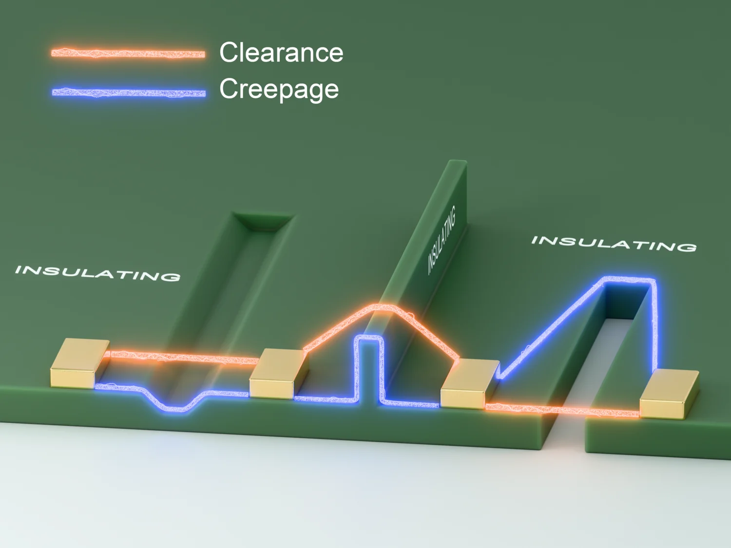
Maximizing Clearance and Creepage Distances
For systems operating at 800V, it is critical to maintain a minimum clearance (the shortest distance through air) of at least 8mm and a creepage distance (the shortest distance along the surface of the insulator) of 10mm between high-voltage traces and connectors. These specifications, guided by standards such as IEC 60664-1, are crucial for significantly reducing the risk of arcing and mitigating partial discharge phenomena.
Strategic Connector Positioning
High-voltage connectors should be strategically positioned near the PCB edges. This placement minimizes the length of high-voltage traces, thereby reducing the potential for interference with other, more sensitive circuits. Furthermore, edge placement simplifies the integration of effective shielding solutions.
Voltage-Level Grouping and Robust Connectors
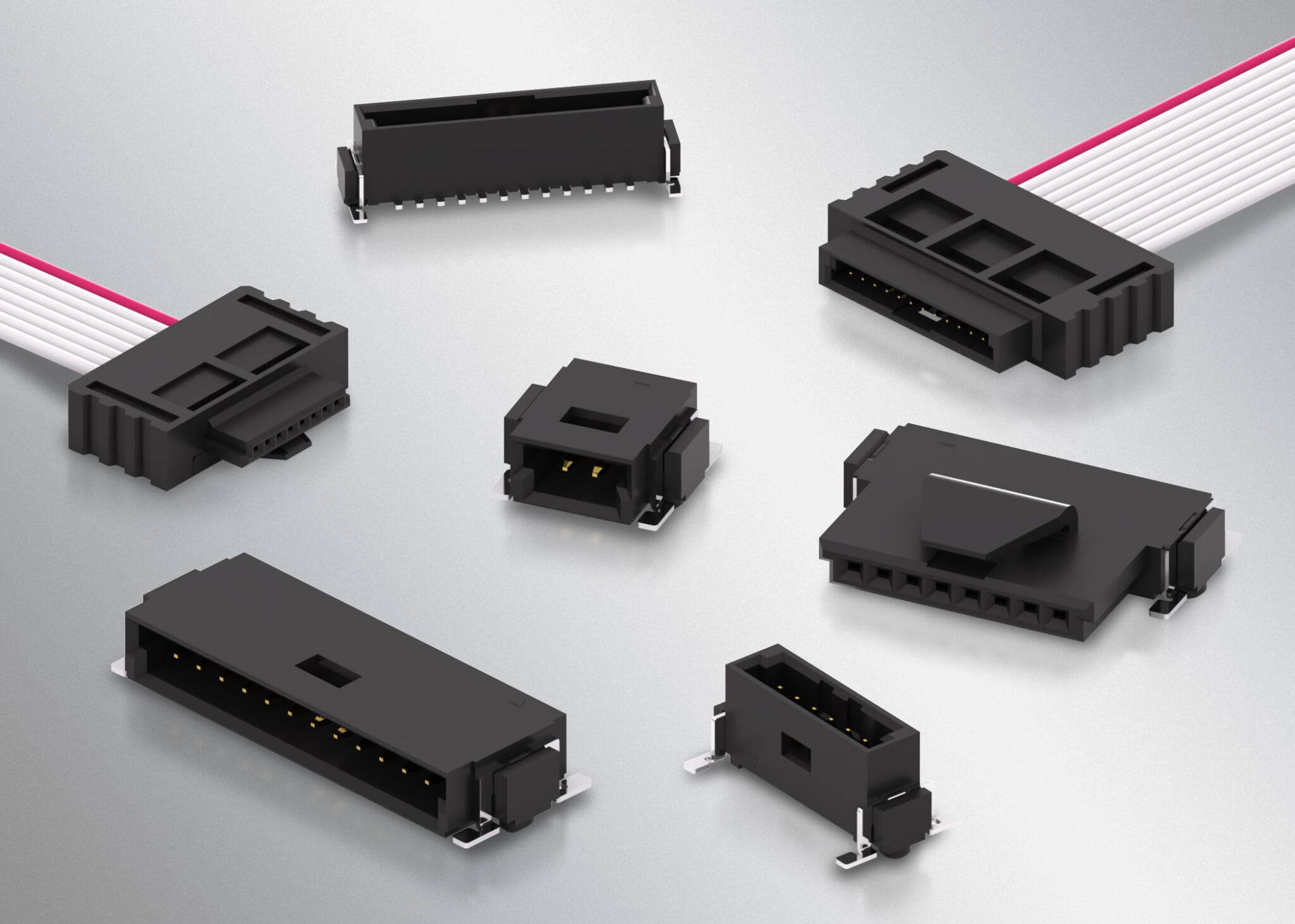
Group high-voltage connectors (e.g., battery input/output) distinctly separate from low-voltage connectors (e.g., communication lines). This segregation prevents crosstalk and ensures proper insulation coordination between different voltage domains. When selecting connectors, opt for robust automotive-grade components specifically rated for high-voltage and high-current applications. Products like TE Connectivity's AMP+ series, capable of handling up to 1000V and 200A, offer the reliability necessary for demanding automotive environments.
Arc Suppression Techniques for High-Voltage PCBs in EV BMS
Electrical arcing represents a significant safety and reliability concern in EV BMS designs due to the inherently high voltages involved. Implementing effective arc suppression techniques is essential to prevent damage and ensure operational safety.
Dielectric Barriers and Conformal Coatings
Incorporate robust insulating materials, such as PCB FR-4 with a high dielectric strength (approximately 20kV/mm), between high-voltage traces and connectors. This physical barrier significantly impedes arc formation. Additionally, applying a conformal coating to the PCB surface, with a dielectric strength of at least 500V/mil, provides crucial protection against moisture and dust—environmental factors that can readily initiate arcing, particularly in humid automotive conditions.
Overvoltage Protection and Trace Geometry Optimization
Integrate transient voltage suppressors (TVS diodes) in close proximity to high-voltage connectors. These components are designed to effectively clamp sudden voltage spikes that could otherwise lead to arcing. For instance, a TVS diode rated for 1000V can provide robust protection against surges in an 800V system. Furthermore, optimize high-voltage trace geometry by avoiding sharp corners. Sharp angles tend to concentrate electric fields, thereby increasing the susceptibility to arcing. Employ rounded corners with a minimum radius of 0.5mm to distribute electric fields more uniformly.
Insulation Coordination and Safety Interlocks: Non-Negotiables for EV BMS
Rigorous insulation coordination and the implementation of robust safety interlocks are absolutely essential in EV BMS to protect both users and maintenance technicians from high-voltage hazards.
Insulation Coordination Guidelines
Insulation coordination ensures that every part of your high-voltage PCB can withstand the specific electrical stresses it will encounter throughout its operational life.
● Material Selection: Choose PCB substrates with high Comparative Tracking Index (CTI) values, such as FR-4 with a CTI of 600. Such materials exhibit superior resistance to surface breakdown under sustained high voltage.
● Multilayer Isolation: In multilayer PCBs, dedicate specific internal layers exclusively to high-voltage traces. These layers should be separated from low-voltage signals by solid ground planes. A typical stack-up for robust insulation might involve a 1.6mm thick board with a minimum dielectric spacing of 0.2mm between critical layers.
● Dielectric Strength Testing: After the design phase, rigorously subject your PCB to Hipot (high potential) testing. This involves applying a voltage 1.5 times the system's operating voltage (e.g., 1200V for an 800V system) to thoroughly verify the integrity of the insulation.
Implementing Safety Interlocks (HVIL)
Safety interlocks are absolutely non-negotiable in EV BMS designs, serving to protect both users and technicians from high-voltage hazards. These systems are engineered to ensure that power is safely disconnected during maintenance procedures or in the event of a fault.
● High-Voltage Interlock Loop (HVIL): Design a dedicated HVIL circuit in close proximity to high-voltage connectors. This loop utilizes low-voltage signals (typically 5V or 12V) to detect if a connector is improperly disengaged. Upon detection, it triggers an immediate shutdown of the high-voltage system.
● Strategic Placement and Shielding: Position HVIL components and their associated traces strategically close to the high-voltage connectors to minimize latency in fault detection. Ensure that traces for interlock signals are adequately shielded to prevent any electromagnetic interference that could compromise their functionality.
● Redundancy for Reliability: For critical connectors, implement dual or redundant interlock circuits. This redundancy ensures that if one circuit fails, the other can still effectively trigger a safe shutdown, thereby meeting stringent automotive safety integrity standards.
Mitigating Partial Discharge in High-Voltage PCBs
Partial discharge (PD) refers to localized electrical discharges that occur within the insulation system of a high-voltage component or at the interfaces between different insulating materials. These small discharges, though often not immediately apparent, gradually degrade materials over time, ultimately leading to catastrophic failure. In EV BMS operating at high voltages, PD is a "silent killer" that must be proactively addressed.
Electric Field Distribution and Insulation Quality
● Smooth Conductor Geometry: Avoid sharp edges or pointed geometries on conductors, as these create highly concentrated electric fields that are prone to initiating PD. Employ field grading techniques, such as adding rounded guard rings around high-voltage pads, to distribute electric fields more uniformly.
● High-Quality Insulation Materials: Select insulation materials with extremely low void content to prevent internal discharges. For example, using epoxy-based conformal coatings with a breakdown strength exceeding 30kV/mm can provide superior PD resistance.
Monitoring and Testing for PD
During the prototyping and testing phases, utilize specialized PD detection equipment to identify any hotspots or areas susceptible to partial discharge on your PCB under actual operating conditions (e.g., 800V at 85°C). Any detected discharges must be addressed by increasing spacing, improving insulation, or refining conductor geometry. By proactively managing PD, you can significantly extend the operational lifespan of your BMS and prevent unexpected field failures.
Choosing the Right Automotive Connectors for EV BMS
The selection of appropriate automotive connectors directly impacts the performance, reliability, and safety of your high-voltage PCB in an EV BMS.
Key Connector Selection Considerations
● Voltage and Current Ratings: Always ensure that connectors are rated significantly above your system's maximum operating voltage and current. For instance, an 800V/100A BMS should utilize connectors rated for at least 1000V/150A to provide a crucial safety margin.
● Environmental Resistance: Automotive connectors must be engineered to withstand severe environmental stresses, including intense vibrations, broad temperature swings (typically -40°C to 125°C), and high humidity. Look for connectors with IP67 or higher ingress protection ratings, offered by reputable manufacturers like Amphenol or Molex.
● EMI Shielding: For high-voltage lines routed near sensitive BMS circuits, utilize connectors with integrated shielding capabilities. This helps to effectively reduce electromagnetic interference and maintain signal integrity.
Practical Tips for Finalizing Your High-Voltage PCB Design
Once you have meticulously addressed connector placement, arc suppression, partial discharge mitigation, insulation coordination, and safety features, these final steps are crucial to ensure your design is fully prepared for production.
● Pre-Prototyping Simulation: Prior to physical prototyping, leverage advanced simulation tools such as Altium Designer or Cadence. These tools allow for detailed analysis of electric field distribution and thermal performance. For example, ensure that no hotspot on the PCB exceeds 125°C under a continuous 100A load.
● Adherence to Automotive Standards: Strictly comply with relevant automotive standards, including AEC-Q100 for component reliability and ISO 16750 for environmental testing. This ensures your design not only meets but often exceeds industry expectations for performance and durability.
● Iterative Testing and Refinement: After constructing a prototype, conduct comprehensive high-voltage stress tests and thermal imaging analyses to identify any latent weaknesses. Be prepared to adjust design parameters, such as increasing trace widths (e.g., from 2mm to 3mm for critical high-current paths) or adjusting spacing, as needed based on empirical test results.
Conclusion: Building Safer, More Reliable EV BMS with Optimized PCB Layouts
Designing an optimal high-voltage PCB layout for EV Battery Management Systems is a complex yet critically important endeavor. By strategically focusing on key areas such as precise connector placement, advanced arc suppression techniques, diligent partial discharge mitigation, robust insulation coordination, and comprehensive safety interlocks, engineers can create systems that are both highly efficient and inherently safe. The judicious selection of appropriate automotive connectors and strict adherence to established industry standards further bolster reliability in the exceptionally demanding conditions characteristic of electric vehicles.
As an engineer, your overarching goal is to meticulously balance cutting-edge performance with uncompromised safety. Utilize the detailed tips and advanced strategies presented in this guide to continuously refine your designs, rigorously simulate performance, and thoroughly test every aspect. By conscientiously applying these fundamental principles, you are not merely designing a PCB; you are actively contributing to the transformative future of sustainable transportation. Let us collectively continue to push the boundaries of EV technology towards new frontiers of safety, efficiency, and innovation.