Why Are SMD Inductors Crucial in Modern PCB Design?
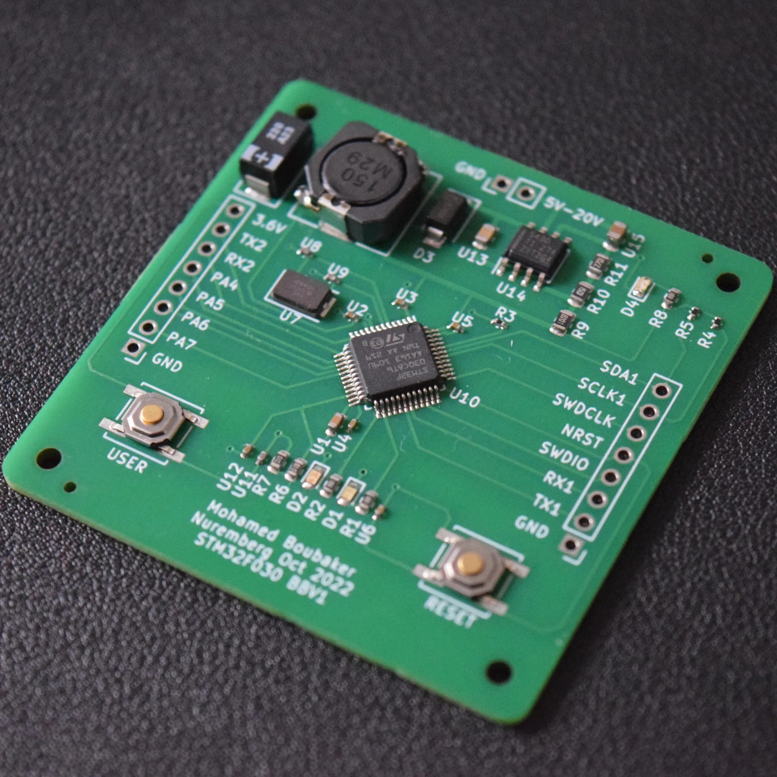
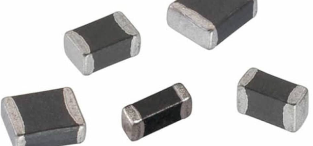
Surface-mount device (SMD) inductors are fundamental components in contemporary electronics, serving vital functions such as energy storage, signal filtering, and suppressing unwanted noise in diverse circuits. They are indispensable in applications ranging from power supply units to advanced radio-frequency (RF) systems. Unlike older through-hole components, SMD inductors are directly soldered onto the surface of a printed circuit board (PCB), making their specific footprint design and precise placement exceptionally important.
The way an inductor's footprint is designed and how it's integrated into the PCB layout profoundly impacts overall circuit performance. Suboptimal design can lead to problems like signal interference, excessive heat generation, or even premature component failure. Adhering to established guidelines for SMD inductor footprints and best practices for PCB layout is therefore essential. These practices ensure that the design not only meets functional specifications but also supports efficient manufacturing and long-term reliability.
What Defines an SMD Inductor Package and Its Footprint?
SMD inductors come in a variety of physical sizes, often identified by numerical codes like 0402, 0603, or 0805, which correspond to their dimensions in inches (e.g., a 0402 package measures 0.04" by 0.02"). However, it's important to note that unlike some other components, inductor package sizes aren't always uniformly standardized across manufacturers. This means that the exact footprint required for an inductor can vary significantly, even for components with the same nominal package size, necessitating a close look at thedatasheet of online pcb manufacturer.
The footprint of an SMD inductor encompasses the copper pads on the PCB where the component will be soldered, along with the corresponding solder mask and solder paste layers. A well-engineered footprint is critical for several reasons: it ensures robust solder joints during assembly, minimizes unwanted parasitic electrical effects, and prevents mechanical stress on the component after installation. When creating a footprint, always consult the recommended land pattern provided in the inductor’s datasheet. If a precise match isn't available in your PCB design software's library, it’s typically a quick process to adjust an existing footprint to align with the datasheet's specific dimensions.
Example Footprint Details
For instance, a standard 0603 inductor might specify a pad width of 0.8 mm and a pad spacing of 1.6 mm. However, these figures are not universal and can differ between manufacturers. Following detailed guidelines is crucial for compatibility with automated assembly equipment and for preventing common soldering issues such as "tombstoning," where one end of the component lifts off its pad during the reflow process.
H2: What Are the Key Design Rules for SMD Inductor Footprints?
Creating an effective footprint for SMD inductors demands meticulous attention to detail. Implementing the following essential guidelines will lay a strong foundation for your surface mount inductor designs.
Pad Dimensions and Solder Layers
It is vital to precisely match the copper pad dimensions and their spacing to the manufacturer’s recommendations. Pads that are too small can lead to inadequate solder joints, while overly large pads might result in excess solder, potentially causing short circuits. The solder mask opening should be slightly larger than the copper pad to facilitate proper solder flow. Concurrently, the solder paste stencil should accurately cover the pad area, ensuring the correct volume of solder paste is deposited—typically covering 90-100% of the pad surface for smaller components.
Clearance and Thermal Relief
Maintain sufficient clearance between the inductor pads and any adjacent traces or other components to prevent unintended short circuits. A minimum clearance of 0.2 mm is often suggested for small inductors, though specific design rules may necessitate variations. For inductors operating in high-current applications, incorporating thermal relief patterns into pads connected to large copper planes is a smart strategy. This practice mitigates heat absorption issues during the soldering process, promoting a reliable and robust solder joint. Adherence to industry standards, such as IPC-7351, which provides detailed specifications for SMD footprints, also ensures manufacturability and design consistency.
How Can You Optimize PCB Layout for Inductor Performance?
Beyond merely designing the footprint, the strategic placement and routing of SMD inductors on a PCB significantly influence overall circuit performance. Inductors are frequently used in sensitive applications, such as switching power regulators, where a poorly planned layout can introduce electromagnetic interference (EMI), noise, or reduce efficiency. Adopting these best practices for inductor PCB layout is crucial.
Strategic Component Placement
Position inductors in close proximity to the components with which they primarily interact, such as integrated circuits (ICs) in a switching regulator circuit. For example, within a buck converter design, the inductor should be placed near the switching node to shorten high-current loops. Shorter loops inherently reduce parasitic inductance and minimize EMI. A good general rule for high-frequency designs (above 1 MHz) is to keep the distance between the inductor and the switching IC under 10 mm.
Minimizing Current Loop Areas
In switching power supplies, the current path involving the inductor, input capacitor, and output capacitor should be kept as compact as possible. Enlarged loop areas act like antennas, radiating EMI that can adversely affect nearby circuits. Whenever feasible, route traces on the same layer, and use vias sparingly to avoid introducing additional inductance. For a two-layer board operating around 500 kHz, strive to keep loop areas under 100 mm².
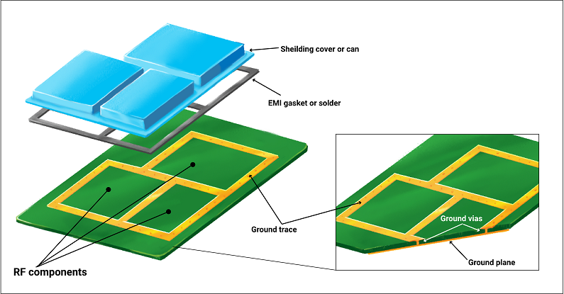
Ground Plane Considerations
While ground planes are essential for noise reduction, their placement underneath inductors requires careful thought. In switching regulator designs, it's generally best to avoid placing a ground plane directly beneath the inductor or the switching node, as this can couple noise directly into the ground. Instead, consider placing the ground plane on an adjacent layer or creating a cutout to isolate these high-noise areas. If a ground plane is unavoidable in such a location, a split plane or cutout can help mitigate noise coupling.
Orientation for EMI Mitigation
Inductors generate magnetic fields that can induce interference in nearby components or signal traces. To minimize this coupling, orient inductors strategically—for instance, placing them perpendicular to sensitive signal traces. In designs incorporating multiple inductors, maintain a spacing of at least 5-10 mm between them to reduce mutual interference, especially if they operate at similar frequencies.
Effective Thermal Management
Inductors used in power applications, particularly those handling high currents (e.g., above 2 Amperes), can generate substantial heat. Ensure there is adequate copper area around the inductor pads to facilitate heat dissipation, and avoid positioning inductors close to heat-sensitive components. In designs of multilayer PCB, incorporating thermal vias near the inductor pads can effectively transfer heat to inner layers, helping to keep component temperatures below their rated limits (often 125°C).

What Are Common Inductor Layout Challenges and Solutions?
Even with meticulous planning, designers frequently encounter specific challenges when integrating SMD inductors into a PCB layout. Understanding these issues and their solutions is key to ensuring design reliability.
Mitigating Parasitic Effects and Soldering Issues
Long traces or large current loop areas can introduce undesirable parasitic inductance and capacitance, which degrade circuit performance, especially in high-frequency circuits (above 1 MHz), where even a 5 mm trace can add around 5 nH of inductance. The solution is to keep traces as short and direct as possible. Soldering defects, such as tombstoning or weak joints, often stem from incorrect pad sizes or improper solder paste application. To address this, always double-check footprint dimensions against the component datasheet and verify that reflow profiles match the inductor’s requirements (e.g., a peak temperature of 260°C for lead-free solder).
Addressing Mechanical Stress and EMI
SMD inductors are susceptible to cracking if subjected to mechanical stress, such as during board flexing. To prevent this, position inductors away from board edges or areas prone to high stress. For rugged applications, consider adding underfill material for extra mechanical support. Electromagnetic interference (EMI) originating from inductor magnetic fields can induce noise in neighboring circuits. Solutions include employing shielding where necessary or increasing the spacing between inductors and sensitive components to at least 10 mm, especially in designs with currents exceeding 1 Ampere. Proactively tackling these challenges during the design phase significantly reduces rework and prevents costly field failures. Utilizing simulation tools, often integrated into PCB design software, for EMI and thermal performance analysis can predict potential issues early on.
How Do You Select the Right SMD Inductor for a Design?
Optimizing the inductor’s footprint and layout works hand-in-hand with selecting the appropriate component. Here are critical factors to consider when choosing an SMD inductor.
Key Selection Criteria
Current Rating: Select an inductor with a current rating that is at least 20-30% higher than your circuit’s maximum operating current to prevent magnetic saturation. For example, a circuit drawing 1 Ampere should ideally use an inductor rated for at least 1.3 Amperes.
Inductance Value: Match the inductance value to the specific needs of your application. Higher values (e.g., 10 µH) are generally suited for lower-frequency power supplies, while lower values (e.g., 1 µH) are often preferred for high-frequency switching applications.
DC Resistance (DCR): For power applications, opt for inductors with low DC resistance (e.g., below 50 mΩ) to minimize energy losses and heat generation, thereby improving efficiency.
Package Size: Ensure the physical package size of the inductor fits within the available space constraints on your board, while also providing an adequate pad area for reliable soldering. Smaller packages, such as 0402, are excellent for compact designs but typically feature lower current ratings compared to their larger counterparts.
Balancing these selection factors with robust inductor PCB layout best practices ensures your design achieves both its performance and long-term reliability objectives.
Crafting Superior PCB Designs Through Optimized Inductor Layouts
Designing effective SMD inductor footprints and carefully planned layouts is a cornerstone for creating high-performing and dependable printed circuit boards. By consistently adhering to established SMD inductor footprint guidelines, implementing best practices for inductor PCB layout, and focusing on precise surface mount inductor footprint design, engineers can significantly reduce issues such as EMI, thermal stress, and soldering defects. Every decision, from selecting the right component to optimizing its placement and routing, directly influences the ultimate success and functionality of your design.
Dedicate sufficient time to thoroughly review manufacturer datasheets, comply with critical industry standards like IPC-7351, and employ simulation tools to analyze potential layout issues before finalizing your design. These proactive strategies will equip you to confidently navigate the complexities of modern PCB design, allowing you to deliver circuits that consistently meet the rigorous demands of today’s compact, high-performance electronic devices.
Begin integrating these principles into your upcoming projects, and observe how your designs achieve enhanced levels of operational efficiency and long-lasting durability. For more valuable insights and resources on PCB design and component selection, continue to follow our blog.