Why Are Embedded Components Transforming PCB Design?
The electronics industry is constantly pushing the boundaries of miniaturization. As devices become more compact, faster, and more powerful, engineers face the complex task of integrating greater functionality into ever-smaller footprints without compromising performance. This challenge has led to a significant innovation: embedded components in PCB design. This approach involves integrating resistors, capacitors, and even active devices directly within the layers of a printed circuit board.
This technique not only conserves valuable board space but also significantly enhances reliability and signal integrity, making it an ideal solution for cutting-edge applications. From discreet wearables to advanced automotive systems, embedded components are fundamentally reshaping how electronic products are conceived and manufactured. This discussion will delve into the latest advancements in this technology and explore practical applications, offering engineers valuable insights to optimize their upcoming projects.
What Defines Embedded Components in PCB Manufacturing?
Understanding Component Integration within PCB Layers
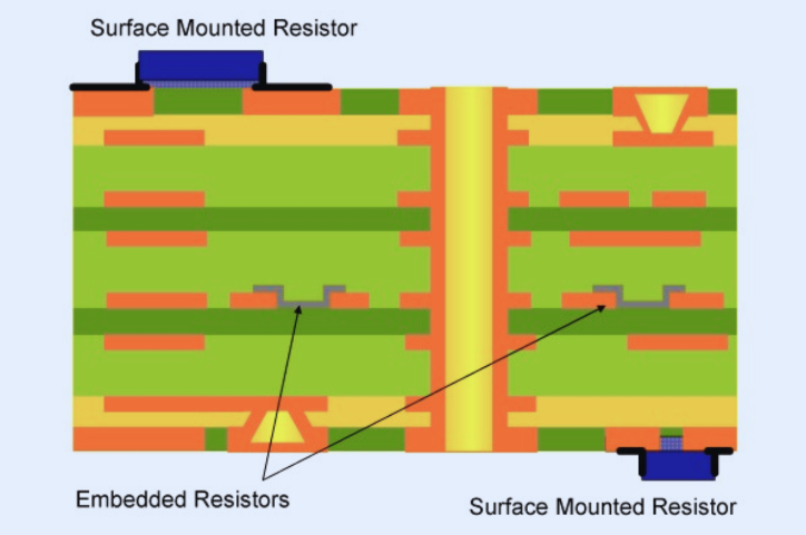
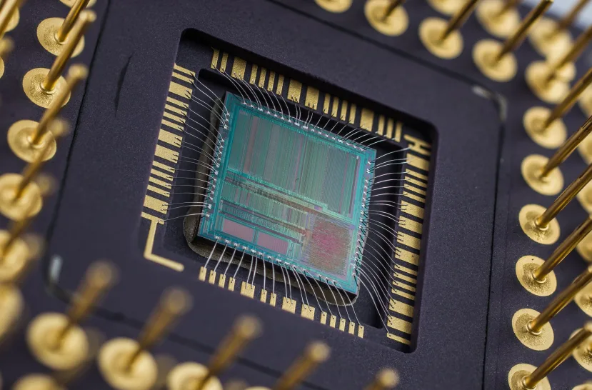
Embedded components refer to electronic parts—such as resistors, capacitors, or even integrated circuits (ICs)—that are placed within the internal layers of a PCB rather than being mounted on its external surfaces. In contrast to conventional surface-mount technology (SMT) or through-hole methods, these components are encased within the board during the fabrication process. This can involve discrete components precisely placed on an inner layer or passive elements that are directly formed within the substrate material itself.
The typical manufacturing sequence begins with the creation of specific cavities or recesses within the PCB layers. Components are then carefully positioned within these cavities and electrically connected using microvias or fine copper traces. For instance, a resistor can be created by depositing a specialized resistive material between copper layers, enabling precise values like 50 ohms with a typical tolerance of ±15%. This method of internal integration significantly reduces the reliance on external solder joints, which can decrease parasitic inductance by as much as 50% compared to traditional SMT, thereby markedly improving overall electrical performance.
How Do Embedded Components Offer a Competitive Edge?
The widespread adoption of embedded components is driven by their ability to address contemporary engineering challenges. This technology provides several key benefits that distinguish it from conventional approaches.
Key Advantages for Modern Electronics
● Significant Space Savings: By integrating components internally, the surface area required on a fast turn custom PCB can be reduced by up to 35%, as demonstrated in compact devices like health trackers. This frees up crucial space, allowing for either increased functionality or more streamlined, aesthetically pleasing designs.
● Superior Signal Integrity: Shorter interconnects inherent to embedded designs drastically reduce parasitic effects. For high-frequency circuits operating between 40–50 GHz, signal loss attributable to embedded resistors is often negligible, sometimes less than 0.1 dB, in comparison to surface-mounted alternatives.
● Enhanced Reliability: Without exposed solder joints, embedded components exhibit greater resilience to mechanical stress from shock, vibration, and extreme temperature fluctuations. This is particularly vital for applications such as automotive electronics, where PCBs may be subjected to thermal cycles reaching 170°C.
● Improved Thermal Management: Heat generated by components dissipates more uniformly across the board, minimizing the formation of localized hot spots. Placing thermal vias near embedded ICs can reduce thermal resistance by 20–30%, thereby extending the component's lifespan.
While these advantages are significant, embedded designs do present certain trade-offs. They can increase manufacturing complexity and associated costs—sometimes by 15–25%—and components are not easily replaced or tested once embedded post-assembly. Nevertheless, for high-performance or compact applications, the benefits often considerably outweigh these limitations.
What Innovations Are Advancing Embedded Component Technology?
The growing prominence of embedded components is not merely a trend; it is propelled by continuous, cutting-edge innovations that enhance their practicality and power. These advancements are making embedded solutions more accessible and robust for a wider range of applications.
Breakthroughs in Fabrication
Advanced fabrication methods, such as precision laser drilling and multi-layer pressing, have revolutionized the way components are embedded. Lasers create cavities with exceptional accuracy, controlling depths to within 10 microns, which ensures a precise fit for each component. For instance, processes like Würth Elektronik's "SOLDER.embedding" technique involve soldering surface-mount devices (SMDs) onto inner layers before integrating them into a multilayer structure, leading to high reliability, especially for demanding automotive applications.
The Role of Microvia Technology
Microvias, which are miniature holes as small as 50 microns in diameter, are essential for connecting embedded components to the outer layers of the HDI PCB. This technology enables extremely dense routing and creates signal paths as short as 0.1 mm, which can reduce parasitic inductance to below 1 nH in certain scenarios. This capability is particularly beneficial for high-density interconnect (HDI) designs, where maximizing every millimeter of board space is crucial.
Evolution of Formed Passives
Beyond embedding discrete parts, a significant innovation is the "forming" of resistors and capacitors directly within the PCB using specialized resistive or dielectric materials. A formed resistor might achieve a base value of 100 ohms with a ±5% tolerance, which can be further adjusted during the etching process to meet highly precise specifications. This method streamlines assembly, reduces component count, and enhances manufacturing consistency.
Wide Bandgap (WBG) Semiconductor Integration
The embedding of Wide Bandgap (WBG) semiconductors, such as silicon carbide (SiC) or gallium nitride (GaN) devices, is increasingly being adopted for power electronics. These WBG materials allow for switching speeds up to 100 kHz. Embedding these components can reduce parasitic inductance by 30–40%, as demonstrated in a 10 kW inverter design developed by Schweizer Electronic, leading to significant performance gains in power conversion.
Where Are Embedded Components Making a Real-World Impact?
While the theoretical advantages are clear, it's in practical applications that embedded components truly demonstrate their transformative power. They are enabling new functionalities and improved performance across diverse industries.
Wearable Health Trackers
Consider a modern fitness band that precisely monitors heart rate and transmits data wirelessly, all within a sleek, lightweight form factor. Embedding resistors and capacitors directly beneath the microcontroller can reduce the PCB size by up to 35%, as shown in a prototype from PCBOnline. Furthermore, these shorter signal paths enhance the reliability of wireless transmission, facilitating stable 2.4 GHz connections with minimal power loss.
Automotive Traction Inverters
Electric vehicles (EVs) rely heavily on highly efficient power conversion systems. Infineon's 1200 V CoolSiC™ MOSFETs, when embedded using Schweizer’s p2PACK® technology, can deliver a 50 kW half-bridge inverter design with notably low thermal impedance. This results in a performance increase of approximately 35% compared to traditional packaging methods, primarily due to reduced switching losses and superior heat dissipation capabilities.
High-Frequency RF Systems
In radio frequency (RF) attenuators tested at frequencies up to 60 GHz, embedded resistors have consistently exhibited excellent performance with minimal signal loss, typically under 0.2 dB. By strategically placing terminating resistors directly beneath a BGA package, engineers have managed to shorten connection lengths to just 0.5 mm. This drastic reduction in length minimizes parasitic capacitance, significantly improving signal integrity for critical 5G applications.
Aerospace Sensor Miniaturization
Miniaturized sensors used in satellite systems greatly benefit from the integration of embedded passives. One particular design, which embedded capacitors within a multilayer PCB, achieved a 20% weight reduction and successfully withstood vibrations up to 50 G, complying with stringent UL and IPC standards. Such compactness is absolutely crucial in aerospace applications where every gram impacts mission efficiency and cost.
What Should Engineers Consider When Designing with Embedded Components?
To successfully integrate embedded components into your next PCB project, careful planning and attention to detail are essential. These practical tips will help ensure optimal performance and manufacturability.
Key Design Considerations
● Precision Placement: Components should be meticulously aligned with die bonds to facilitate direct connections. A misalignment of as little as 25 microns can increase resistance by 10%, highlighting the need for CAD tools capable of maintaining tight tolerances.
● Comprehensive Thermal Planning: For high-power components, incorporating thermal vias nearby is critical. For instance, 4–6 vias, each 0.3 mm in diameter, can reduce the thermal resistance of a 1W resistor by approximately 25%.
● Tolerance Management: Embedded resistors typically exhibit a tolerance of 15–20% due to variations in the etching process. Designs should account for this by maintaining consistent impedance—for example, 50 ohms across all traces—to preserve overall performance.
● Early Manufacturability Consultation: It is crucial to engage with your fabricator early in the design phase. Quick-turn prototyping (1–3 days) is generally not feasible for embedded designs, so plan for extended lead times, typically ranging from 5–7 days.
Following these guidelines will help maximize the potential of embedded technology while proactively mitigating common design and manufacturing pitfalls.
What Are the Challenges and Future Trends for Embedded Components?
Despite their considerable promise, embedded components still face several hurdles that influence their broader adoption. Addressing these challenges will be key to unlocking their full potential.
Existing Challenges
The higher upfront costs associated with embedded designs—sometimes as much as 20% more than traditional SMT solutions—can be a deterrent for projects with tight budgets. Testing also presents greater complexity; once a component is embedded, a faulty capacitor, for instance, cannot be easily replaced without potentially scrapping the entire board. Furthermore, while innovations like microvia embedding are progressing, scaling these advanced techniques for high-volume mass production remains an ongoing challenge.
Future Outlook
Looking ahead, the trajectory of embedded technology points towards further evolution with greater 3D integration and a stronger alignment with the demands of the Internet of Things (IoT). Analysts predict that by 2030, embedded components will be utilized in 50% of all HDI PCBs, driven by the increasing need for smarter, smaller, and more integrated devices. Advances in materials, such as FR4 alternatives with improved thermal conductivity (e.g., 0.5 W/mK), are expected to further boost performance and contribute to cost reductions.
How AIVON Supports Advanced Embedded Component Designs
For engineers engaged in projects utilizing embedded components, partnering with a proficient manufacturer is absolutely vital. AIVON offers state-of-the-art manufacturing capabilities specifically tailored for these complex designs. This includes quick-turn prototyping, achievable in as little as 5 days, and precise HDI fabrication featuring microvias as fine as 50 microns. Our global logistics network ensures efficient and timely delivery, while our dedicated one-on-one engineering support helps refine your designs for optimal manufacturability. Whether you're optimizing a 100-ohm embedded resistor or integrating a sophisticated SiC module, AIVON's expertise, backed by certifications like ISO 9001:2015 and IPC-A-600 Class 3, is geared to bring your innovative PCB concepts to fruition.
Conclusion
Embedded components in PCB design represent more than just an industry trend—they signify a fundamental shift in how electronic devices are conceived and engineered. By significantly conserving space, enhancing electrical performance, and opening up entirely new design possibilities, this technology is powering a vast array of devices, from discreet wearables to cutting-edge electric vehicles. Ongoing innovations, such as advanced microvia technology and the integration of wide bandgap semiconductors, are continually pushing the boundaries of what’s possible, with real-world applications consistently demonstrating their tangible value. For engineers, mastering this technology involves carefully balancing its numerous benefits against considerations like increased costs and design complexity. However, the resulting gains in functionality and reliability invariably justify the effort. As we advance towards a future characterized by smarter, more compact, and interconnected devices, embedded components will undoubtedly remain at the core of the next wave of technological breakthroughs. Are you ready to integrate this transformative approach into your designs? AIVON is here to assist you in making it a reality.