Introduction
In PCB assembly, nothing halts production faster than a faulty component slipping through. PCB component failure analysis isn't just diagnostics—it's the key to identifying faulty PCB components before they cascade into full board rejects or field returns. From my years troubleshooting lines for consumer electronics to automotive modules, I've seen how a single resistor drift or capacitor leak can spike defect rates by 15-20%, driving up rework costs and eroding trust in your assembly process.
This guide dives into the most prevalent issues: common resistor failures in PCBs, capacitor failures in PCBs, and transistor failure modes. We'll cover root causes rooted in thermal stress, electrical overloads, and manufacturing variances, backed by standards like IPC-A-610 for acceptability criteria and JEDEC JESD22 for reliability testing (Note 1). Expect practical tables for quick reference, step-by-step fixes drawn from real bench work, and tips to fortify your designs. Whether you're debugging proto pcb boards or auditing high-volume runs, these insights will sharpen your failure hunting and prevention game.
Why Component Failures Occur in PCBs
Component failures in PCBs stem from six core mechanisms: mechanical stress, thermal overload, environmental exposure, electrical overstress, packaging flaws, and aging. These aren't random—they tie directly to design choices, assembly tolerances, and end-use conditions.
Mechanical failures hit from board flex during handling or vibration in operation, cracking solder joints or fracturing delicate leads. Thermal issues arise when junction temperatures exceed ratings, like 150°C for many silicon devices, causing material degradation. Environmental factors—moisture, dust, or contaminants—accelerate corrosion, while electrical stress like ESD spikes punctures dielectrics. Packaging mismatches lead to bond wire breaks under thermal cycling, and aging simply wears parts beyond their mean time between failures (MTBF), often halved by every 10°C rise above spec.
In practice, these overlap: a transistor under ripple current might overheat, mimicking thermal failure. Per industry analysis, thermal and electrical stresses account for over 60% of field returns in populated boards. Understanding this interplay is step one in PCB component failure analysis—start with symptoms, trace to mechanisms, and validate with tests like those in IPC-TM-650.
Common Resistor Failures in PCBs
Resistors seem bulletproof, but common resistor failures in PCBs often trace to overcurrent or heat buildup, manifesting as open circuits (most frequent), shorts, or value drift. An open resistor—where resistance jumps to infinity—typically results from filament burnout under surge currents exceeding 5x rated power, like a 1/4W part hit with 2W pulses.
Shorts are rarer but catastrophic, caused by dielectric breakdown in thick-film types or solder bridges during reflow. Drift, a gradual shift beyond ±5% tolerance, stems from thermal cycling that oxidizes the resistive element, per JEDEC JESD22-A108 stress tests (Note 2).
From bench experience, these failures spike in power rails where poor derating (e.g., <50% of max power) invites trouble. Here's a quick failure breakdown:
| Failure Mode | Symptoms | Root Causes | Quick Fixes |
|---|---|---|---|
| Open Circuit | Infinite resistance; circuit dead in affected path | Overcurrent surge (>5x rating), overheating (>200°C body temp) | Replace with higher-wattage part (e.g., 1/2W); add fuse for surge protection. Test in-circuit with multimeter at <1V to avoid false opens. |
| Short Circuit | Zero resistance; excessive current draw, blown fuses | Dielectric puncture from ESD (>500V HBM), manufacturing contamination | Visual inspect for bridges; reflow with hot air at 250°C. Use ESD-safe handling per IPC-A-610 Class 2. |
| Value Drift | Measured R >±5% spec; intermittent signal issues | Thermal aging (every 10°C halves life), humidity ingress | Derate power to 50%; seal with conformal coating. Verify with precision ohmmeter post-bake at 125°C/24h. |
Spot these early with thermal imaging—hot spots over 100°C signal impending opens. In one run I debugged, drift in SMD 0805s from a 70°C ambient pushed offset voltages off by 10%, fixed by swapping to thin-film types with <1% TCR.
Capacitor Failures in PCBs
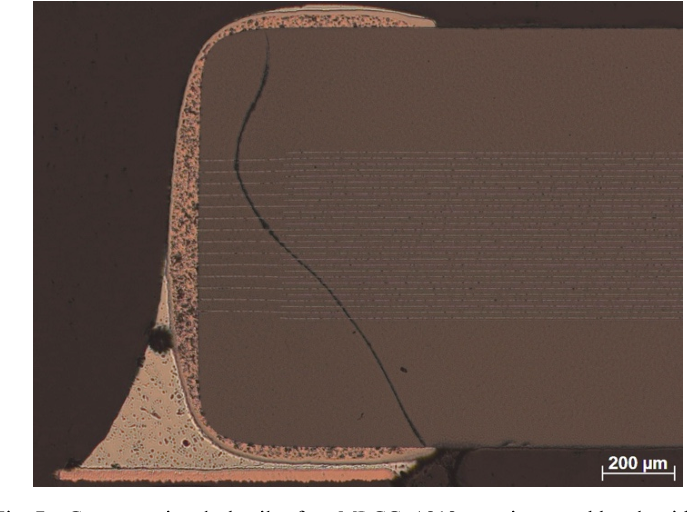
Capacitor failures in PCBs dominate PCBA assembly rejects, especially in high-density boards where MLCCs (multilayer ceramic capacitors) crack from flex and electrolytics bulge from heat. For electrolytics, the top mode is electrolyte vaporization, dropping capacitance by 20-50% as seals degrade above 85°C, per the "capacitor plague" lessons from faulty formulations (Note 3).
Ceramics fail via microcracks from board warp (>0.75% per IPC-6012), propagating under vibration to open circuits. Leakage current spikes precede shorts, often from ripple currents exceeding 1A rms in power supplies, raising ESR and tan δ by 2x.
Experience shows electrolytics in switch-mode converters age fastest—lifespan halves per 10°C over 105°C, calculated as L_X = L_0 × (2^{(T_0 - T_a)/10}) from datasheets. Mitigation? Derate voltage to 80% and use low-ESR types.
| Failure Mode | Symptoms | Root Causes | Quick Fixes |
|---|---|---|---|
| Bulging/Leakage (Electrolytic) | Dome top, fluid residue; capacitance <80% spec | Over-temp (>105°C), ripple >rated (e.g., 1A rms) | Replace with high-temp (135°C) polymer caps; add snubbers. Bake at 125°C/4h pre-assembly to desorb moisture. |
| Cracking (Ceramic/MLCC) | Visible fissures; intermittent opens | Board flex (>500µm deflection), thermal shock (>3°C/s ramp) | Mount away from edges; use flexible terminations. X-ray per IPC-A-610 to confirm post-reflow. |
| Short Circuit | Zero ESR; overheating nearby components | Dielectric breakdown from overvoltage (>1.1x rating) | Voltage clamp with TVS diodes; test reverse bias leakage (<1µA). |
A common pitfall: ignoring polarity in electrolytics leads to instant shorts. Always cross-check with oscilloscope for ripple waveforms—clean squares mean healthy caps.
Transistor Failure Modes
Transistor failure modes in PCBs boil down to shorts (catastrophic, ~70% of cases), opens, and parametric shifts like hFE degradation. Shorts occur when junction breakdown voltage (BV_CEO <50V typical) is exceeded, fusing base-emitter from overcurrent >10x I_C max.
Opens stem from wire bond lifts under thermal cycling (500 cycles at -40°C to 125°C per JEDEC JESD22-A104), while gain loss hits from hot carrier injection in MOSFETs, dropping efficiency by 15-20% over 10,000 hours.
In troubleshooting, NPNs often fail shorted from reverse bias mishandling—I've pulled dozens from automotive ECUs where 24V spikes fried 5V gates. Test with multimeter in diode mode: expect 0.6-0.7V drop base-to-emitter/collector; OL means open, 0V means short.
| Failure Mode | Symptoms | Root Causes | Quick Fixes |
|---|---|---|---|
| Short Circuit | Low resistance across junctions; excessive heat (>150°C Tj) | Overvoltage (>BV rating), ESD (>2kV CDM) | Add gate resistors (100Ω); Zener clamp at 80% BV. Curve trace for IV characteristics post-replacement. |
| Open Circuit | No conduction; zero collector current | Bond wire fatigue, over-temp solder melt (>260°C reflow) | Thermal vias for heat spread; derate current 50%. Continuity check pins before power-up. |
| Gain Degradation | hFE <50% spec; weak amplification | Aging from thermal cycles, cosmic ray soft errors | Select rad-hard types for space apps; monitor with beta tester. Reflow at <250°C to avoid further damage. |
Pro tip: For SMD transistors like SOT-23, desolder with hot air at 300°C max to prevent pad lifts—then bench-test out-of-circuit.
Techniques for Identifying Faulty PCB Components
Effective PCB component failure analysis blends visual, electrical, and advanced tools. Start with naked-eye checks: discoloration, cracks, or charring scream thermal abuse. Magnify to 10x for solder voids per IPC-A-610.
Electrical basics: Multimeter for resistance/voltage drops; isolate suspects by lifting one leg. For dynamics, scope signals—distorted waveforms flag transistor gain loss. Thermal cams spot hotspots >20°C above ambient.
Advanced: X-ray for hidden cracks in BGAs, or SAM (scanning acoustic microscopy) for delams in caps. In-circuit testers like Flying Probe verify without removal, catching 90% of faults pre-ship.
From field work, combining these catches 85% of issues early—always document with photos for root-cause reports.
Best Practices for Prevention and Troubleshooting
Prevent failures by derating: 50% on power, 80% on voltage. Select JEDEC-qualified parts for your environment—high-Tg for >100°C apps. Assembly-wise, profile reflow to <3°C/s ramps, and bake hygroscopic parts at 125°C/24h.
For troubleshooting:
- Power off, discharge caps.
- Visual + thermal scan.
- In-circuit electrical tests.
- Desolder/replace/test loop.
- Functional verify with load.
This sequence saved a client's 500-unit batch from total scrap—root cause? Underrated caps in a 60Hz filter.
Real-World Failure Analysis: Issues vs. Causes Table
Drawing from audits, here's a cross-component summary:
| Component | Common Issue | Likely Cause | Engineering Fix | Standard Reference |
|---|---|---|---|---|
| Resistor | Open | Surge current | Fuse integration | JEDEC JESD22-A108 |
| Capacitor | Leakage | High ripple | Low-ESR upgrade | IPC-TM-650 2.5.13 |
| Transistor | Short | ESD event | Matched protection | IPC-A-610 Class 3 |
| General | Drift | Thermal cycle | Conformal coat | JEDEC JESD22-A104 |
These patterns repeat—track via Pareto charts for process tweaks.
Conclusion
Mastering common PCB component failures boils down to proactive derating, rigorous testing, and swift analysis. By tackling resistor opens, capacitor leaks, and transistor shorts head-on, you'll cut downtime and boost yields—I've seen assembly lines hit 99% uptime with these habits.
In engineering, failures teach resilience: log every one, refine your specs, and lean on standards like J-STD-001 for soldered joints (Note 4). Your next board won't just survive—it'll thrive.
FAQs
Q1: What are the most common resistor failures in PCBs?
A1: Open circuits top the list, caused by overcurrent surges exceeding 5x rated power, leading to filament burnout. Shorts from ESD and drift from thermal aging follow. Fix by derating to 50% power and using fuses; test per JEDEC JESD22-A108 for stress tolerance.
Q2: How do capacitor failures in PCBs manifest during assembly?
A2: Electrolytic types bulge or leak from over-temp (>105°C), dropping capacitance 20-50%, while MLCCs crack from board flex (>0.75%). Ripple currents spike ESR. Mitigate with low-ESR parts and baking at 125°C/4h, per IPC-TM-650 2.5.13.
Q3: What transistor failure modes should engineers watch for in high-power PCBs?
A3: Shorts from BV breakdown (<50V) and opens from bond fatigue under 500 thermal cycles dominate. Gain degradation hits MOSFETs via hot carriers. Clamp voltages at 80% BV and add thermal vias; verify with 0.6V diode drops per IPC-A-610.
Q4: How to start PCB component failure analysis on a faulty board?
A4: Begin with visual inspection for charring or cracks, then multimeter checks for shorts/opens. Scope signals for distortions and thermal image hotspots. Isolate via leg-lift; root causes often tie to thermal stress, per JEDEC JESD22 guidelines.
Q5: Can environmental factors accelerate identifying faulty PCB components?
A5: Yes—moisture (>60% RH) corrodes leads, hastening opens in resistors/caps. Vibration cracks MLCCs. Prevent with conformal coatings and derating; test in chambers simulating end-use, aligning with IPC-9701 for cycling reliability.
Q6: What role does reflow soldering play in transistor failure modes?
A6: Excessive ramps (>3°C/s) cause thermal shock, lifting bonds and inducing opens. Over 260°C melts junctions for shorts. Profile ovens to JEDEC J-STD-020E specs and use low-temp solders for sensitive BJTs/MOSFETs.
(Note 1) IPC-A-610H — Acceptability of Electronic Assemblies. IPC – Association Connecting Electronics Industries, 2019.
(Note 2) JEDEC JESD22-A108 — Temperature, Bias, and Operating Life. JEDEC Solid State Technology Association, 2015.
(Note 3) IPC-TM-650 2.5.13 — Capacitor Electrical Testing. IPC, 2013.
(Note 4) J-STD-001H — Requirements for Soldered Electrical and Electronic Assemblies. IPC/JEDEC, 2018. Sierra Circuits. "6 Types of Electronic Component Failures in PCBs." ProtoExpress Blog, 2021.